EsperanzaL
Newbie level 3
Hello,
I am quite new to layout and I am using IBM technologies.
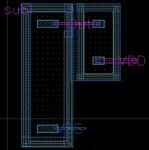
In my circuit I have several resistors and fets. Let me take the nwell resistor as an example. The schematic view takes this resistor as a three terminal device, and I connect the body to subc. But LVS indicates discrepancies for all these resistors. I have one p+ contact in the layout, and these are the only LVS errors for this circuit.
The netlist created for the layout seem to be incorrect.
In the source netlist (schematic), I would have
Rnwres2 net2 VSS sub! $[nwres] m=1 r=1.72743K w=3.93u l=10u par=1 sbar=1 mSwitch=0
While in the layout netlist, the resistor becomes
R2 VSS 4 1727.43 L=1e-5 W=3.93e-6 sbar=1 par=1 $SUB=sub! $[nwres] $X=-3360 $Y=210 $D=247
Does anyone know how to fix this problem?
Thanks in advance.
