Welcome to our site! EDAboard.com is an international Electronics Discussion Forum focused on EDA software, circuits, schematics, books, theory, papers, asic, pld, 8051, DSP, Network, RF, Analog Design, PCB, Service Manuals... and a whole lot more! To participate you need to register. Registration is free. Click here to register now.
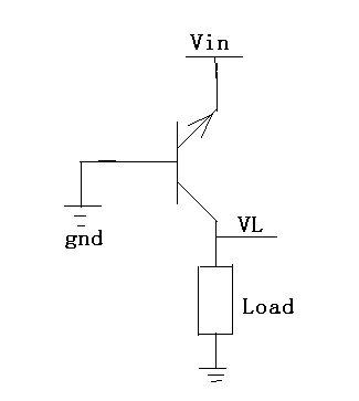
It's a base stage, like the upper part of a cascode stage (drawn upside down). Could serve as an impedance converter (low input impedance, high output impedance (Rout=Rload)), but for relatively small signal only: The emitter being at -0.7V (in case of Si), the collector could have something in between, say -0.45V, hence the max. output swing could be something like ± 200 .. 250mV . It has some voltage gain, current gain ≤ 1, no phase inversion.
The low input impedance would suggest an Iin rather than a Vin label at the node apparently intended as input. Also Vin must be negative related to gnd(and would be typically drawn near the schematic bottom).
It's hard to decide, if the circuit is dedicated to the purpose analyzed by erikl or just a drawing artefact... Using pnp instead of npn wouldn't change anything, except voltage and current polarity.
This site uses cookies to help personalise content, tailor your experience and to keep you logged in if you register.
By continuing to use this site, you are consenting to our use of cookies.