Continue to Site

Welcome to EDAboard.com

Welcome to our site! EDAboard.com is an international Electronics Discussion Forum focused on EDA software, circuits, schematics, books, theory, papers, asic, pld, 8051, DSP, Network, RF, Analog Design, PCB, Service Manuals... and a whole lot more! To participate you need to register. Registration is free. Click here to register now.

Not getting triggered in Vivado logic analyzer

Status
Not open for further replies.

rahdirs

Advanced Member level 1
Joined
May 22, 2013
Messages
424
Helped
93
Reputation
192
Reaction score
91
Trophy points
1,308
Location
Mordor
Activity points
4,492
Hi,

I am debugging a part of my design which involves writing & reading from a DDR3 using MIG ip.
So i inserted debug cores from netlist.(Mark Debug-> Set up Debug core etc...)
In initial test i only wanted to debug,what i'm writing & what i'm reading back:
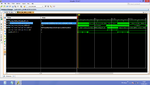
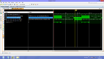
My debug probes-

ila0
1) app_wdf_data
2) app_cmd
3) rd_en (giving write data through a fifo,so fifo's rd_en)

ila1
1) app_rd_data
2) app_rd_data_valid

After programming virtex 7,logic when ila0 gets triggered is:
when rd_en == '1' & app_cmd == '0'.
This is working fine,i'm seeing the data which needs to be written.

when ila1 needs to be triggered,
when app_rd_data_valid == '1'.

Here is the issue.When you set a condition & select trigger it waits for the trigger by showing a hour-glass icon on debug probes window & when it occurs waveform is generated.
But in this case,when i set the logic & click trigger it says in TCL "ila1 armed at time ...." but then there is no hour-glass icon on debug probes & no waveform.

Usually when clk/signal is not attached to debug port it throws up a error/warning here there is nothing except that tcl command ila1 armed ................

I am pretty much new to debugging a design via chipscope,logic analyzer etc..
 

Did you try the Trig Immediate button on ila1. If nothing happens, probably the clk is not running. Is both ila share the same clk?

Another possibility is to include the default debug core from the MIG. When generating the MIG, you can add the debug core to the memory core.

I hope that it helps.
 

If nothing happens, probably the clk is not running. Is both ila share the same clk?
.
If the clk is not running-it shows a pop up error :- Core clock either too slow or not connected.
In vivado if the 2 clks are same,it groups them under a single debug port.No both have different clocks.

Will try that MIG debug core.
 

Another possibility is to include the default debug core from the MIG. When generating the MIG, you can add the debug core to the memory core.
I hope that it helps.

That default debug core you were saying which is an option while generating MIG in the GUI,is it only for debugging example design or can you use it to debug custom DDR Designs as well ?
 

Okay I had to rebuild a design I'm working on and I let a free running counter in the design, which I was originally sampling with a much higher frequency clock be placed in its own ILA (on its generating clock), so I have something similar to what you have. Enabling triggering on both ILAs worked perfectly using 2014.3.

I'm not sure why you are having this issue. Unfortunately I wouldn't be able to even try out your design as I don't have a eval board. Perhaps you can try a build with two counters running on different clocks that rollover in 10's of seconds so you can enable both triggers and see if that works just to prove that it's not Vivado's hardware manager that is having a problem.

Are you sure app_rd_data_valid is being sampled in the ILA with the correct clock domain?
 

Are you sure app_rd_data_valid is being sampled in the ILA with the correct clock domain?

The signal is being sampled with correct clock domain but that trigger condition never meets,so that issue is present.My query about lack of hour glass icon might be - that the logic analyzer has finished the process of collecting data,so i'm not seeing the icon.

The thread is being kept alive as i am waiting for Tetik's reply to post# 4

This might seem like I'm treating you like you don't know anything, but that's not the intention...

Did you start both ILAs? You need to press the run trigger on both ILA tabs, otherwise they won't both be running at the same time.

Each ILA will trigger and open it's own waveform window.
 

This might seem like I'm treating you like you don't know anything, but that's not the intention...
Did you start both ILAs? You need to press the run trigger on both ILA tabs, otherwise they won't both be running at the same time.
Each ILA will trigger and open it's own waveform window.
This was the topic of thread,on pressing ila option on both ILA hardware dashboards,the first ila was giving waveform & the second wasn't ?

The signal is being sampled with correct clock domain but that trigger condition never meets,so that issue is present
I just saw my reply in post #6,i meant that trigger condition(APP_RD_DATA_VALID = '1') was not being met,so it's not getting asserted to '1' & remains '0',so no waveform is being plotted. :D
 

I just saw my reply in post #6,i meant that trigger condition(APP_RD_DATA_VALID = '1') was not being met,so it's not getting asserted to '1' & remains '0',so no waveform is being plotted. :D

So this seems more like there is a design problem and the APP_RD_DATA_VALID doesn't go active. Have you run a simulation of the design or did you just jump right into debugging on hardware (I assumed you had run a simulation of the design)?
 

So this seems more like there is a design problem and the APP_RD_DATA_VALID doesn't go active. Have you run a simulation of the design or did you just jump right into debugging on hardware (I assumed you had run a simulation of the design)?

The simulation works fine.Able to write into & read back from DDR3.

After a few failed debug trials on hardware,i simplified my fsm logic so that 1 only do a burst write,wait & then read back.

I also changed the ila clock of app_rd_data & app_rd_data_valid so that it has same clock as other ila(now write & read signals in same ila).As my sample depth in ila is large - 4096 ,i can see both write & read commands being given in same window,then i saw that read valid doesn't go high when i gave read command & read data stays at "00...0".

Then i programmed example design given by xilinx with a few modifications to check for board issues but it works fine.

Now i'm guessing either i'm not following timing diagram given in manual(but then why does it work in simulation) or i'm writing a lot of addresses back to back before reading(sounds silly)
Snapshot of my design debug waveform:

Untitled.png
 
Last edited:

I would probably run the example design simulation and concentrate on looking at how the app_rd_* side signaling protocol, and compare that with your design. I suspect you'll find a difference in the protocol between the two.

You did run the simulation with a DDR3 model, right? It didn't report any problems, correct? And you read back the values you wrote?

You're talking about following read timing diagrams ? Yeah,that is what i feel i should do,check if i'm following the read timing diagrams the way xilinx expects.

Yes did run with DDR3 model,a MICRON ddr3 model,who also provide the ddr3 on my board as well
 

My guess is the DDR3 didn't calibrate for some reason. (resets/power/dci/io/constraints/etc...) You can see your attempt to write because you generate it. It didn't sound like you probed further down to see if it actually worked.
 

My guess is the DDR3 didn't calibrate for some reason. (resets/power/dci/io/constraints/etc...) You can see your attempt to write because you generate it. It didn't sound like you probed further down to see if it actually worked.

In my code,i have a UART interface.I need to change the value of some signal after MIG calibration is done.So the calib_complete signal that is an o/p of MIG which indicates whether calibration is done,i store it in a read only register.So i've seen in UART,calib_complete signal does go high indicating no issues from hardware side.
Anyway i've also debugged example_design code on my board & it shows no failure from hardware side.

Anyway,the code is working now.Earlier i was writing 1500 addresses back to back & reading them back.Now i have reduced the number to 300 writes at a time.It's working now.Maybe there is a limit to the number of addresses you can write at once.
 

Attachments

  • Custom_run_3.png
    Custom_run_3.png
    75.7 KB · Views: 91
  • Custom_run_8.png
    Custom_run_8.png
    79.2 KB · Views: 126

Status
Not open for further replies.

Part and Inventory Search

Welcome to EDABoard.com

Sponsor

Back
Top