Continue to Site

Welcome to EDAboard.com

Welcome to our site! EDAboard.com is an international Electronics Discussion Forum focused on EDA software, circuits, schematics, books, theory, papers, asic, pld, 8051, DSP, Network, RF, Analog Design, PCB, Service Manuals... and a whole lot more! To participate you need to register. Registration is free. Click here to register now.

NOR gate simulation hspice

Status
Not open for further replies.

erman_wellem

Newbie level 5
Joined
Jun 12, 2009
Messages
8
Helped
0
Reputation
0
Reaction score
0
Trophy points
1,281
Activity points
1,338
Hi,

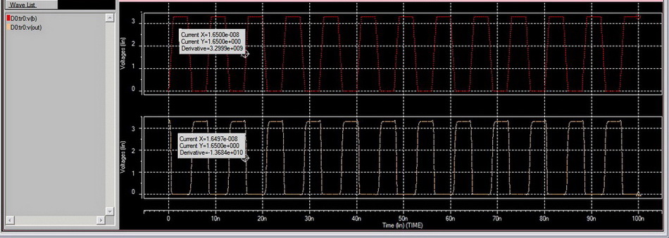
I'm doing a simulation of a CMOS NOR gate using hspice and
want measure tplh and tphl from input A to the output. The input signal to A is a pulse waveform swing from 0 to 3.3V, input B is 0V. It seems ok and work fine. I can get the tplh and tphl

The problem is when the condition is reversed (Input A is 0V and input B is pulse). I want to measure the tplh and tphl from input B to output. I got the value of tphl is negative. tplh is positive (its OK).

I know in NOR gate the t_plh and t_phl usually not symmetric. the tplh is greater than tphl. But in my opinion, tphl should NOT a negative value.

Anyone have idea about this? Thanks
 

How are you "measuring" it? Have you viewed the output waveforms? If so, maybe you can post them. The output cannot change before the input!

Keith.
 

Hi Keith,

Thanks for response. I measure it using the statements below

.TRAN 0.01ns 100ns
* Measure delay from input B to output OUT
.MEASURE TRAN tPHL TRIG V(B) VAL=1.65 RISE=3 TARG V(OUT) VAL=1.65 FALL=3
.MEASURE TRAN tPLH TRIG V(B) VAL=1.65 FALL=3 TARG V(OUT) VAL=1.65 RISE=3
.MEASURE TRAN tPD PARAM='(tPHL + tPLH)/2'

The NOR gate has a capacitor as its load. Also, the W/L of PMOS and NMOS are the same. I guess this W/L values affect the tplh and tphl. Am I correct?
 

You certainly need to look at the output waveforms to see what is happening. I don't use Hspice so I don't know what your measuring command syntax is, but if the 3 is looking for the time of the 3rd edge then the problem may be that you need to measure from the 3rd to the 4th, not 3rd to 3rd.

While the transistor sizing will affect tphl and tplh, it cannot make it negative.

Keith
 

tphl can't be negative!!

Please post your graphical output screen and layout.
 

Hi,

It is not from a layout, only a simple SPICE file. Here is the output waveform


The red one is input B and the other is the output. As you can see from the measurement, the X value in output waveform is smaller than X value in the input waveform. The value of Y is 1.65 (VDD/2)

The width and length of PMOS and NMOS are the same. I tried to change the width of PMOS to be 1um greater than the width of NMOS while keeping the L the same. Now the tplh is positive. So, my temporary conclusion is: we can not design NOR gate using PMOS and NMOS with the same W/L. PMOS should have a greater width. Is it correct? Thanks for help
 

One problem I see is your input slope is very slow. The gate could start to switch at Vth above Vss, long before the input reaches mid rail. Try a faster rise/fall time on the input.

Keith.
 
HI
I HAVE SOME SUGGESTION
WHEN U R TALKING ABOUT tpphl + or negative ,it is ahppening because u r measure command is reading wrong value. so befor u write measure commnd jsut check when u r going to measure i.e rise 1.2.3 and fall 1. 2 3. then decide to measure it
as fas as simulation of same W/L is concerned it will work
 

Status
Not open for further replies.

Part and Inventory Search

Welcome to EDABoard.com

Sponsor

Back
Top