Continue to Site

Welcome to EDAboard.com

Welcome to our site! EDAboard.com is an international Electronics Discussion Forum focused on EDA software, circuits, schematics, books, theory, papers, asic, pld, 8051, DSP, Network, RF, Analog Design, PCB, Service Manuals... and a whole lot more! To participate you need to register. Registration is free. Click here to register now.

Non-inverting AC amplifier

Status
Not open for further replies.

bhl777

Full Member level 6
Joined
Sep 30, 2008
Messages
363
Helped
0
Reputation
0
Reaction score
0
Trophy points
1,296
Activity points
5,140
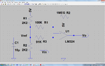
Hi everyone, I have a question about this circuit. I suppose C1 is used to remove DC of Vin, but how can we know the value of R3? It seems like we do not need R3 for calculating Vout/Vin, why it is there? Thank you!
200961523135686.gif
 

The feedback connections are both made to the inverting (-) input. The non-inverting input (+) is grounded through a resistor. This is what forces the inverting input to be a virtual ground: the amplifier output voltage depends on the voltage difference between the two inputs, rather than the absolute voltage at either input.

Because the input transistors inside the op amp do actually require a very slight input current, there is a very slight corresponding voltage drop across the resistors connected to those inputs. However, if the resistor connected to the non-inverting input is approximately the same as the parallel combination of Rin and Rf, the resulting voltage drops will be the same and will tend to cancel each other out.

Source: **broken link removed**

C1 is used to remove DC of Vin >>> TRUE

KAK
 

Apart from the points, that have been already explained, the shown circuit doesn't work correctly as a linear amplifier, because it misses a negative supply voltage respectively a suitable input bias.
 
  • Like
Reactions: bhl777

    bhl777

    Points: 2
    Helpful Answer Positive Rating
Single-Supply Op-Amp Circuit Collection

**broken link removed**

look pict 1 & 2 and read text 1.1 , 1.2 and 1.3

KAK
 

Hi FvM, do you think this diagram is correct for non-inverting AC amplifier? Thank you! 1.png
Apart from the points, that have been already explained, the shown circuit doesn't work correctly as a linear amplifier, because it misses a negative supply voltage respectively a suitable input bias.
 

The amplifier of the post #1 is absolutely wrong for LM107 though it is copied from the datasheet. The reason was already pointed out by FvM. V- shouldn't be tied to ground because the lowest amplitude of Vin needs to be higher than V- about 2V typically (in case of LM107).
It seems you tried in your amplifier of (post #5) creating a virtual ground so that you can use a single supply. It doesn't matter it is also wrong but since you thought about it I think you are ready to get the answer rather easily.
Usually (if not always), the bias of an opamp is set at its IN+. Its other input IN- will follow it automatically while the opamp output is not saturated. So let us assume we have a supply 0-5V and we like to set the virtual ground of an opamp as LM324 at 2.5V (actually I choose 1.8V since its output limit is 5-1.4=3.6V). As you did on your schematic we add a divider R+R and if necessary we bypass its mid node by a capacitor C. This node (Vref) will be our virtual ground. It is not recommended to connect it directly to IN+.

Suppose we like to insert Vin at IN+ (to get a non-inverting amplifier). Its gain will be (1 + R2/R1) but R1 should be connect between IN- and ground (virtual in our case). This means R1 should be connected to Vref. So Vref and IN+ should be isolated first by a resistor, say R3. Its value is made, as possible, be equal to R2//R1 (for DC balance as explained in a previous post). Note that R3 is also imporatnt even the opamp will run as an inverting amplifier only. On the othet hand, we usually let R be much smaller than the resistors which are connected to Vref, or if there is an extra opamp, it will be used as a non-inverting unity gain buffer (no R1).

R3 will be the load for Vin source assuming R<<R3 and for AC, the bypass capacitor could help if R not too small.

Kerim
 

Attachments

  • NonInverting_01.png
    NonInverting_01.png
    103.2 KB · Views: 100
Last edited:
  • Like
Reactions: bhl777

    bhl777

    Points: 2
    Helpful Answer Positive Rating
Hello KerimF, could you tell me again which part of the diagram in #5 is wrong? Since I saw your answer now, I didn't find out where should I need to revise. Thank you for your advise!
The amplifier of the post #1 is absolutely wrong for LM107 though it is copied from the datasheet. The reason was already pointed out by FvM. V- shouldn't be tied to ground because the lowest amplitude of Vin needs to be higher than V- about 2V typically (in case of LM107).
It seems you tried in your amplifier of (post #5) creating a virtual ground so that you can use a single supply. It doesn't matter it is also wrong but since you thought about it I think you are ready to get the answer rather easily.
Usually (if not always), the bias of an opamp is set at its IN+. Its other input IN- will follow it automatically while the opamp output is not saturated. So let us assume we have a supply 0-5V and we like to set the virtual ground of an opamp as LM324 at 2.5V (actually I choose 1.8V since its output limit is 5-1.4=3.6V). As you did on your schematic we add a divider R+R and if necessary we bypass its mid node by a capacitor C. This node will be our virtual ground. For a few reasons, it is not recommeded to connect it directly to IN+.

To be continued...
 

Hello KerimF, could you tell me again which part of the diagram in #5 is wrong? Since I saw your answer now, I didn't find out where should I need to revise. Thank you for your advise!

The circuitry at the pos. input is correct.
The feedback to the neg. input should consist of the classical resistive voltage divider (to set the gain) - however, it must be tied to ground via a large capacitor.
As a consequence, the dc gain is unity (as required for single supply operation) and the required ac gain is established only above the corner frequency set by the capacitors.
 
  • Like
Reactions: bhl777

    bhl777

    Points: 2
    Helpful Answer Positive Rating
which part of the diagram in #5 is wrong?
It misses a feedback voltage divider. The negative OP inout is shorted to ground, AC-wise. As a result, the amplifier is operated with the OP open-loop gain, if C is suffcient large.

You can add a resistor between the negative OP input and the bias circuit, similar the the schematic in post #6. Or replace the RRC circuit by a RC series circuit, as suggested by LvW
 
  • Like
Reactions: bhl777

    bhl777

    Points: 2
    Helpful Answer Positive Rating
Status
Not open for further replies.

Part and Inventory Search

Welcome to EDABoard.com

Sponsor

Back
Top