Continue to Site

Welcome to EDAboard.com

Welcome to our site! EDAboard.com is an international Electronics Discussion Forum focused on EDA software, circuits, schematics, books, theory, papers, asic, pld, 8051, DSP, Network, RF, Analog Design, PCB, Service Manuals... and a whole lot more! To participate you need to register. Registration is free. Click here to register now.

noise on micro controller pwm output

Status
Not open for further replies.

mshh

Full Member level 6
Joined
May 30, 2010
Messages
349
Helped
0
Reputation
0
Reaction score
0
Trophy points
1,296
Location
usa
Activity points
3,871
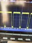
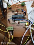
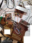
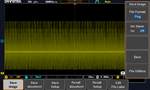
I used mega8 ADC to control duty cycle of pwm output but there is a little noise on pwm signal. I tried to reduce it using 100nf capacitor on inputs, there is caacitor on VCC. there is 1uf on AVref. the external crystal with its two capacitors are close to the mega. the noise increased when connect it to switch dc dc converter.I use the output voltage of the converter as analog input to the ADC of the mega, Is this the noise source?( because of ripple in dc converter) , How to reduce it?
 

Please show the exact schematic and layout you are using. Noise problems can be caused by many things, this sounds like it is either supply or ground noise so layout is important. If you can show a photograph it would help a lot.

Brian.
 

Unlikely that the pwm output is sourcing the noise. It's the power switch driven by the pwm output.
 

This is the noise and it disappeared when I use single pwm output
 

Attachments

  • IMG_20201214_084400.jpg
    IMG_20201214_084400.jpg
    1.1 MB · Views: 138

Check FFT of that signal and try to get a frequency of that noise. Is it perhaps the same frequency as internal clock of your dc/dc converter?
 

Hi,

Show us a photo with the power supply, complete wiring, PCB and scope connections.

Klaus
 

this is schematic diagram MCU pwm control two cascaded converters and board connections attached.

the PC power supply is the only source of this circuit.
 

Attachments

  • boost converter.PDF
    16.4 KB · Views: 98
  • IMG_20201214_085404.jpg
    IMG_20201214_085404.jpg
    1.8 MB · Views: 156
  • 2.jpg
    2.jpg
    364.4 KB · Views: 135
Last edited:

Since all are powered by a single power supply, noise is created when input and output share the common gnd thus either use separate power supply or use dc/dc converter in series with input.

I hope it helps.
 

Hi,

seeing your pictures I´m not surprised that there is noise.
I rather am surprised that it works at all.

Switching power electronics need careful signal wiring.
Very short traces (wires) rather 10mm than 10 cm, low impedance (thick wiring does not mean low impedance), GND planes on PCBs, start point GND wiring, avoiding GND loops, avoiding GND bounce ....
A forum can´t teach all this in a thread.. it will be a longer and intensive process of learning.
You use parts like IR2112 and MOSFETs ... designed for switch mode operation.
--> Go to their internet sites and look for design notes and application notes. All big companies provide a lot of very good documents. They are free. Use this. Maybe you don´t understand every detail of the application notes fro the beginning. This is quite normal

--> For the hardware I recommend to design (at least) all power circuitry on one PCB. The smaller the better (for my taste). One central point where all GND refer to (star GND wiring). And keep on the application notes.

Klaus
 

I am trying to cascade two converters regardless of their type or function. there are stability problems due to cascading converters and i am working on it. now this is the output of the boost converter when coupled to the buck converter, how ever each converter work fine on its own.these noise doesn't appear on computer with ni daq.
 

Attachments

  • DS0001.PNG
    DS0001.PNG
    105.9 KB · Views: 146

Status
Not open for further replies.

Similar threads

Part and Inventory Search

Welcome to EDABoard.com

Sponsor

Back
Top