Continue to Site

Welcome to EDAboard.com

Welcome to our site! EDAboard.com is an international Electronics Discussion Forum focused on EDA software, circuits, schematics, books, theory, papers, asic, pld, 8051, DSP, Network, RF, Analog Design, PCB, Service Manuals... and a whole lot more! To participate you need to register. Registration is free. Click here to register now.

Noise at the comparator output

navbp

Junior Member level 1
Joined
Aug 7, 2012
Messages
19
Helped
1
Reputation
2
Reaction score
0
Trophy points
1,281
Activity points
1,529
Hi,
I need help with a circuit using two comparators (LM2903YPT) to identify overvoltage and undervoltage conditions on 12V supply.

If the supply voltage is within a certain range, the output shall be pulled up to 5V.
But if the supply voltage is out of the specified range, the output shall be pulled low by the open collector comparators LM2903.

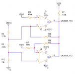
The circuit diagram is attached.

The simulation works fine. As per simulation,
The undervoltage threshold trigger is 10.35V and 11.2V (due to hysteresis).
The overvoltage threshold trigger is 13.285V and 13.45V (due to hysteresis).

Between 11.2V to 13.2V, the LM2903 output is high according to simulation.

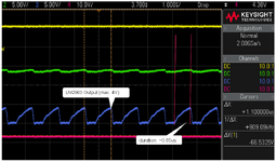
But in reality, noise is observed at the output of LM2903.
The problem is when the supply voltage is near the undervoltage or overvoltage thresholds.
When the VDD12 supply is within the correct range, then the circuit works as expected.
When the VDD12 supply is very low or very high away from the threshold, then the circuit works as expected.
But noise of ~900kHz is observed at the output of the LM2903. The hysteresis is considered but even then, the noise is observed when VDD12 is near these threshold values.

The screenshot of the observed noise is attached.

Please help me to understand what is the reason for this noise and how to correct the circuit.

Thank you.
 

Attachments

  • Supply_Monitoring.png
    Supply_Monitoring.png
    34.9 KB · Views: 165
  • Supply_Monitoring_Waveform.png
    Supply_Monitoring_Waveform.png
    170.9 KB · Views: 105
Hi,
noise is observed at the output
Then most probably there is noise at at the input at first place.
I see no noise filtering in the whole circuit.

Noise is something random.
But in your case it is not really random: It repeats, thus it´s an oscillation.

I often say: I circuit without capacitors isn´t a reliably working circuit.
Capacitors used as noise filters but also used for power supply stabilisation.
None I see.

Also we don´t see the PCB layout. Wrong GND routing may also cause oscillation problems.

And we don´t see what your scope pictures show (just one channel is named), and we don´t see where you connected the according scope_GND to the PCB_GND.

This is why many simulations don't show the realit (..and thus I call useless). They expect perfect PCB layout, expect perfect power supplies, expect no noise...


Klaus
 
Hi,

Then most probably there is noise at at the input at first place.
I see no noise filtering in the whole circuit.

Noise is something random.
But in your case it is not really random: It repeats, thus it´s an oscillation.

I often say: I circuit without capacitors isn´t a reliably working circuit.
Capacitors used as noise filters but also used for power supply stabilisation.
None I see.

Also we don´t see the PCB layout. Wrong GND routing may also cause oscillation problems.

And we don´t see what your scope pictures show (just one channel is named), and we don´t see where you connected the according scope_GND to the PCB_GND.

This is why many simulations don't show the realit (..and thus I call useless). They expect perfect PCB layout, expect perfect power supplies, expect no noise...


Klaus
Thanks for the quick reply KlausST.

There is a bypass cap on the board at the supply of the comparator LM2903YPT.
VDD5 is generated from an onboard LDO and its quite stable. There is cap of >10uF at VDD5 net.
There are provisions to add caps to filter the noise at U4 pin 3, U4 pin 2 and U3 pin 3. But these caps were not populated initially.
So, I have tried adding filter cap at one of these pins, but it didnt solve the issue.

I didnt want to solve this issue by trial and error. but rather understand what is reason for these oscillations.
So, stopped trying to add caps.

Regarding the screenshot from the scope,
Green channel is waveform at U4 pin 2.
Yellow channel is waveform at VDD12.
The scope GND is connected to the PCB GND, which is close to LM2903 GND.
The other signals uses the same GND reference and no oscillations were observed in the GND or in other signals.

Regarding the issues in the PCB, Yes, This is under evaluation.
But, the same circuit was prepared with a general purpose PCB after this issue was observed and got same result.
So, I think it may not be PCB specific.

Regarding simulation, I learnt the hard way. I will be careful next time.

One question: Can we short the output of LM2903YPT as done in this circuit? Is there any impact on the LM2903 functionality if two outputs are shorted?

Thanks,
Navbp
 
Hi,

textual description can´t replace schematics and PCB layout.
Also "10uF" isn´t complete information. If it´s a 10uF electrolytics then it´s usually not suitable for frequencies of 900kHz.

--> Please provide complete information.


Klaus
 
The 2903 output is open collector, and can be tied together which creates a logical "AND"
functionality.

Look at your supply rails, 12V then 5V, set scope to infinite persistence, and see what pk-pk noise looks
like on both those rails. You can also trigger single shot on pulse width to see what is happening on
inputs when output produces HF noise. Scope probes on 10x to minimize Cload.

Not shown do you have large Cload on output ?

Because of ESR issues you might consider a combo of ceramic disk, .1 uF. and an electrolytic
on comparator supply pins. You might be able to get away w/o electrolytic as there are no
large transient currents unless you have large Cload.

You have 100K R's used for +fdbk, and with stray C they can create a lot of phase shift.

One thought, because of layout considerations, plus some internal comparator coupling
cause an unstable loop ? Also good switching performance occurs when there is plenty
of comparator overdrive, 100 mV discussed in data sheet.


Regards, Dana.
--- Updated ---

Some more ap info :


Regards, Dana.
 
Last edited:
You can add a low-pass filter to the output of the comparator. A low-pass filter can reduce high-frequency noise and help smooth out the output signal.
 
Ground noise from output switching can wrap around through the
divider network to the inputs, and there's your phase shift oscillator.
You need hysteresis to be both larger and faster-acting than the
"noise" (more like undesirable circuit response, it is not random)
amplitude seen at the pins.
 
Hi,

textual description can´t replace schematics and PCB layout.
Also "10uF" isn´t complete information. If it´s a 10uF electrolytics then it´s usually not suitable for frequencies of 900kHz.

--> Please provide complete information.


Klaus
Hi Klaus,
3x ceramic 4.7uF and one 47nF is placed at VDD5 net.

@Others: Will consider all these feedback and reply which one worked.
 
Last edited:
A thing to try, is putting a series resistor from the output (and
its pullup if any, which should be attached as tight as possible)
to any driven load or test point. This will "kill" the too-strong HL
transition which bangs the ground, before it can do so. At least
limit it to 5mA peak, or so (as a "5mA" output at a few hundred
mV rated VOL, will have up to 10X that as peak available, and
sharp).

Thee might be trades with net prop delay and any driven-device
input-fall-time sensitivities, because as usual there's a delivery
charge on your free lunch.
 

LaTeX Commands Quick-Menu:

Part and Inventory Search

Welcome to EDABoard.com

Sponsor

Back
Top