Continue to Site

Welcome to EDAboard.com

Welcome to our site! EDAboard.com is an international Electronics Discussion Forum focused on EDA software, circuits, schematics, books, theory, papers, asic, pld, 8051, DSP, Network, RF, Analog Design, PCB, Service Manuals... and a whole lot more! To participate you need to register. Registration is free. Click here to register now.

[SOLVED] NMOS IV characteristic completely different with 2 similar setup

Status
Not open for further replies.

henry kissinger

Member level 2
Joined
Nov 19, 2021
Messages
44
Helped
0
Reputation
0
Reaction score
0
Trophy points
6
Activity points
442
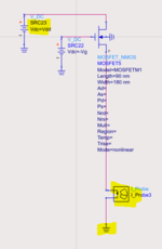
I am plotting the IV characteristics of the NMOS of 2 similar setups.

Here I sweep the Vg from -13 to 13V and vdd from 0 to 50.

note that the only difference is that vdd is positive for one but negative for the other. both grounded at the other end.

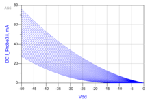
But why I am getting 2 different IV characteristic results? should't they be the same? Shouldn't that Id curve should be only related to difference in drain and source voltages when nmos is turned on with same Vg?
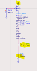
 

Attachments

  • 8ikujyh.PNG
    8ikujyh.PNG
    23 KB · Views: 83
  • kiuyjhtgr.PNG
    kiuyjhtgr.PNG
    17.8 KB · Views: 75
  • oikujyhtgh7j8.PNG
    oikujyhtgh7j8.PNG
    26.7 KB · Views: 87
  • u76hyth5.PNG
    u76hyth5.PNG
    19.7 KB · Views: 87

\[ V_{gs} > 0 \] condition must be maintained.
MOS Transistors may be symmetric on layout but not in model.Therefore they remarked "Source" and the others.
We also don't know that the MOS transistors are Depletion Mode or Enhancement Mode ?
 

Switching Vds polarity means switching drain and source. Respectively Vgs is not the same for both setups.
 

Status
Not open for further replies.

Part and Inventory Search

Welcome to EDABoard.com

Sponsor

Back
Top