Continue to Site

Welcome to EDAboard.com

Welcome to our site! EDAboard.com is an international Electronics Discussion Forum focused on EDA software, circuits, schematics, books, theory, papers, asic, pld, 8051, DSP, Network, RF, Analog Design, PCB, Service Manuals... and a whole lot more! To participate you need to register. Registration is free. Click here to register now.

NMOS Current Mirror Query in Differential Amplifiers

Status
Not open for further replies.

analog_curious

Member level 2
Joined
Feb 17, 2012
Messages
46
Helped
3
Reputation
6
Reaction score
3
Trophy points
1,288
Location
Ireland
Activity points
1,682
All,
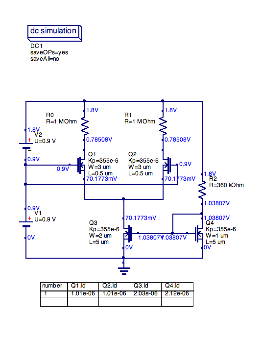
I have a differential amplifier with resistive load. I biased the diff. amp by a tail current source which carries 2*Id (Id is for each side of the input NMOS transistor). Then I tried replacing this tail current source by a NMOS current mirror which gives the same output current as my required current realized through current source.

The issue I am facing is that I am not able to get the same current through my current mirror configuration when I connect it to the source end of my input NMOS circuit. I realize the reason because the Vds is not the same anymore in my current mirror and so I dont see the current I want

I see many circuits online implemented with NMOS current mirrors for NMOS input transistors of differential stage in which they use a separate DC bias at the gate to realise the same Vds condition for current mirror. But then the biasing is dependent on threshold voltage of input transistors.It shouldnt be the case for current mirrors usually right?

Did I understand wrong or..?

Guidances and suggestions are welcome

Dan
 

i think i understand your problem but is there anyway you can draw up a circuit, maybe even draw it on paper and upload the image, if you are separating the output by a differential amp, then the resistive load should not affect the current, but in a current mirror with nmos fets, as long as its hooked up correctly you should be seeing the same current. (also the fets have to have the same Vtn and ((w/l)*un*Cox)
 
Hi
Thanks
I attach the circuit with this
 

Attachments

  • diff_amp.png
    diff_amp.png
    126.4 KB · Views: 141

For this i am going to name the transistors from left to right, and from top to bottom, Q1, Q2, Q3, Q4.

I am reading through your first post and its tough without naming each transistor. Regardless i noticed in your circuit picture that
you are not guaranteeing that Q3 is in Saturation region where Q4 has to be in saturation. if you could explain your problem again but this time
use the Q1-Q4. sorry to take so long on my reply
 
ok i will follow the same naming topology
the current mirror(Q3 and Q4) should be in saturation for the current mirror to work operately..isnt it..Q4 is obviously always in saturation in this case as Vds of it always bigger than its Vgs by a threshold.

i am not sure about Q3's region of operation which was exactly the reason why i got the doubt. If I supply some drain voltage for Q3 through Q1 then ,my current depends on the voltage(Vds3 should be equal to Vds4 for me to get the expected current, 2Id here) there which is not ok for current mirror in general as the current should only depend on the dimensions of the device.

If i understand it right, I should be giving Vdd to the gate of Q1 to have the same Vds3 as Vds4..Is it right or..?

Pardon me if its trivial to ask this. I just dont understand it.

Dan
 
Last edited:

Here's an example in a 0.18µm technology. As you can see, you cannot count on a doubling of current with a doubling of width, if you have such different Vds for Q3 & Q4 :

 
if you supply Vdd to the gate of Q1 or Q2 the transistors will operate in triode region because Vgs1 - Vtn (given) < Vds is the condition for
saturation. Vg - Vs - Vtn < Vd - Vs, (Vs cancel) .... Vg - Vtn < Vd, since there is a resistor in the drain for Q1/Q2, unless the current is very small, then this will not guarantee Q1/Q2 in saturation which would make the current mirror not work. I believe i have this right, dont take this as fact its just what i am suggesting
 
Thanks for the suggestions
So I should probably supply a DC voltage source at the input stage as well along with the current mirror with appropriate width as per my requirement.
I am doing this to replace the ideal current source which I had before instead of current mirror (its is to be mentioned that there is no DC bias supplied at the gate when an ideal tail current source was used)

Am I getting this right or...

Dan
 

So I should probably supply a DC voltage source at the input stage ...

Usually you get this DC voltage by DC feedBack from a further (following) stage.

... as well along with the current mirror with appropriate width as per my requirement. I am doing this to replace the ideal current source which I had before

Yes. Adapt the width (of Q3) for the required current.

Am I getting this right
Yes!
 
Hello

if the voltage drop at the resistors are high ( due to high resistors value ) then the lift voltage for the transistor Q3(current source under differential) will be below the minimum voltage that it need, so I am expecting you are getting less current than what you need. when you work with the current mirror you have to know the minimum voltage and before this voltage the circuit will not perform right. with an ideal current source you will not have this problem because the ideal current source regulate the current with zero needed voltage

I suggest you to use less resistors value although I know it will reduce your gain,
 

Status
Not open for further replies.

Similar threads

Part and Inventory Search

Welcome to EDABoard.com

Sponsor

Back
Top