Continue to Site

Welcome to EDAboard.com

Welcome to our site! EDAboard.com is an international Electronics Discussion Forum focused on EDA software, circuits, schematics, books, theory, papers, asic, pld, 8051, DSP, Network, RF, Analog Design, PCB, Service Manuals... and a whole lot more! To participate you need to register. Registration is free. Click here to register now.

Newbie designed PCB crosstalk problem: 5MHz clk cross coupled to GND

Status
Not open for further replies.

wandola

Junior Member level 3
Joined
Jul 20, 2005
Messages
31
Helped
0
Reputation
0
Reaction score
0
Trophy points
1,286
Activity points
1,554
I am a newbie. I designed a PCB without any supervision 'cause I have nobody to consult.

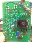
It is a 4-layer PCB to test a ADC chip. The PCB is shown below.

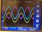
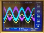
I found that my differential AC signals to the ADC input have been distorted. I think the clk signal is coupled to the the ground plane first. Then coupled to other part of the circuit.

Indeed, the power supply, the LDO output, and even ground plane are all distorted by a periodic signal which is in accordance with the clk.

Is there anything I can do to solve this problem? Or I have to redesign a new PCB...


Pls help the newbie...
 

Attachments

  • pcb.JPG
    pcb.JPG
    2.4 MB · Views: 104
  • input signal to ADC when clk is off.JPG
    input signal to ADC when clk is off.JPG
    142.5 KB · Views: 136
  • input signal become noisy when clk is on.JPG
    input signal become noisy when clk is on.JPG
    745 KB · Views: 129

Statement like below suggest, that you have in the first place a problem of probing your circuit correctly. I don't believe any of your measurements.
Indeed, the power supply, the LDO output, and even ground plane are all distorted by a periodic signal

Nevertheless there may be real clock-to-signal crosstalk. But the differential signalling should eliminate it in a first order for the ADC interface. If the said 5 MHz is the ADC clock, you would see the interference at worst as a DC offset.
 

Out of curiosity, do you have one gnd plane for both digital and analog, or two split planes?
How do you generate clock signal (in what standard) and how they are distributed?
I'm not really an expert, but trying to understand why it happens...
 

Status
Not open for further replies.

Part and Inventory Search

Welcome to EDABoard.com

Sponsor

Back
Top