Continue to Site

Welcome to EDAboard.com

Welcome to our site! EDAboard.com is an international Electronics Discussion Forum focused on EDA software, circuits, schematics, books, theory, papers, asic, pld, 8051, DSP, Network, RF, Analog Design, PCB, Service Manuals... and a whole lot more! To participate you need to register. Registration is free. Click here to register now.

Neutral point clamped inverter: driver ir2110 problem

Status
Not open for further replies.

xVoid

Newbie level 1
Joined
Feb 11, 2015
Messages
1
Helped
0
Reputation
0
Reaction score
0
Trophy points
1
Activity points
36
2011102020581570.jpg
934749_823850271009217_2332409927136870582_n.jpg

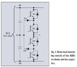
g1,g2 ....... onn ...... +ve voltage
g2,g3 .......onn........ 0 zero voltage
g3,g4 ........onn ....... -ve voltage

it is the switching theme..!

hi i have attached the above diagrams of NPC inverter topology the basic question is about the attachment of the driver ic ir2110 i think two ir2110 ic are required the two above mosfets should have the HIN of the ir 2110 ic and the lower mosfets should have LIN from respective driver ic ... then the basic issue which arises there is that can the driver circuit independently help in driving the two high side mosfets .. with the HIN1 and HIN2 (as there are two driver ic).

and the ground of the circuit should be the ground of the npc or there needs to be some other implementation making the ground of one driver the npc ground and connecting the other ir 2110 ground to the negative side of npc... was just assuming ..!

even tough i will upload one proteus file showing the circuit will u please help in its driver connection..! :-D
 

hello
I am designing the same. I designed the driver circuit but I did not implement it yet. we can discuss if you want.
 

If you are going to try and use this gate driver, then separate isolated 15V feeds to the non grounded switches would be a good idea...!
 

Good idea according to the design I will use three 15v supplies with separate grounds for each IR. so IR1 will supply Q1 and Q3, IR2 will supply Q2 and Q4.
 

you can get high side chips only.... you can't use the lower part of a 2110 on any device other than the single grounded switch, you have to use only the high side parts of the 2110 for the rest.....(i.e. 3 x 2110 required)
 
I simulated the attached design (2 x 2110), please check the results

IR2110.PNGplot.PNG
 

The circuit can't be right. You have multiple switch nodes shorted by GND symbols.

As a first step you should remove all shorts form your schematic.

Presuming you have DC- tied to low voltage ground, than the upper two switches can't be controlled by a regular bootstrap driver.
 

To say simply you can't ground this places

IR2110.PNG

and also there is no third supply point Vn or V0.
 

specifically those two grounds are isolated from IC ground. the simulation results seems ok by LTSpice. for each IC I have three isolated +15 sources. please check the design as per attached below,3.PNG

I am online with simulator so any test required?
 

O.K., that's a completely different circuit than the LTSpice schematic.
 

just look to the IR2110, can it work like that. I think the problem of LTSpice simulator that we can not isolate the grounds. for real simulation I should have the facility to isolate grounds but I can not find a way. is there any tricky way to do that.
 

it will be interesting to see if the upper 2110 works correctly.... it does rely somewhat on the lower o/p section being connected to a node with no dv/dt
 

There is no more Bootstrapping, Actually its possible to put 4 more transistors and you can eliminate IR2110 with use of optocouplers. but still the IR2110 will give the better switching experience.

It would be better with 1k gate discharge resistors in all the IGBT, otherwise there is a chance of damaging the whole circuit.
 
I must use IR for switching delay facility as you are fully aware. I am not trusting LTSpice for that schematic because I am not sure that it has a grounding isolation facility in simulator. two weeks ago, I contacted IR for advise and they are so reluctance to give help as the NPC application is not included/test.
 

this is the simulation when I removed the first GND point (upper). Bootstrapping is clear. as I expected it is a capability of simulator.

Green: HO
Yellow: Vs


a3.PNG
 

As you already have isolated gate driver supplies for each switch, I would probably use optocoupled gate drivers or optocouplers + single channel gate drivers. I don't see any advantage of using the IR2110 level shift feature in this circuit. But using this driver brings up additional failure scenarios, e.g. by undershoot of the VS node.
 

The only advantage of using IR is the internal delay which prevent Q3 from being on while Q1 is turning off. In other words Q3 will conducts only when Q1 is totally off.
 

I cannot see how a model of the 2110 can be so accurate that it takes into account the dv/dt experienced by the internal level shift circuitry when the Vout low side is pulled down rapidly by virtue of the fet it is connected to switching on...this is the difference between real world silicon and a black box model... as the above posters say, if using the opto-couplers there is now no real advantage in using the 2110 any more...
 

I cannot see how a model of the 2110 can be so accurate that it takes into account the dv/dt experienced by the internal level shift circuitry when the Vout low side is pulled down rapidly by virtue of the fet it is connected to switching on...this is the difference between real world silicon and a black box model... as the above posters say, if using the opto-couplers there is now no real advantage in using the 2110 any more...

true except for the delay time. using opto-coupler with TIP122 transistor has also led to IGBT failure. so, the most important feature of IR21xx is its internal delay between HO and LO.
still on my opinion that IR2110 is the only secured option to drive the NPC scheme.
 

using opto-coupler with TIP122 transistor has also led to IGBT failure

Can you show us the circuit you used? when you do the proper timing then what is the point in relying on some external unknown delay?
 

Status
Not open for further replies.

Similar threads

Part and Inventory Search

Welcome to EDABoard.com

Sponsor

Back
Top