Continue to Site

Welcome to EDAboard.com

Welcome to our site! EDAboard.com is an international Electronics Discussion Forum focused on EDA software, circuits, schematics, books, theory, papers, asic, pld, 8051, DSP, Network, RF, Analog Design, PCB, Service Manuals... and a whole lot more! To participate you need to register. Registration is free. Click here to register now.

[SOLVED] Negative Logic gates, when are they used and why?

Status
Not open for further replies.

danny davis

Banned
Joined
Mar 1, 2013
Messages
627
Helped
0
Reputation
0
Reaction score
0
Trophy points
1,296
Location
Hollywood
Activity points
0
On schematics at my job, they use circles on the inputs of gates , what are the names for these types of negative logic gates?

They aren't called AND, OR, NAND, NOR, Exclusive OR or NOR, they have different names , what are they called?

When would a circuit or in general want to use Negative Logic gates?

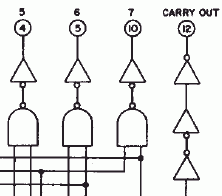
The Negative logic gates have internal inverter buffers on the input that are internally inside the IC Chip

Basic Negative Logic tricks:
1.) You can use input inverter buffers before an OR gate to make to make a NAND gate
2.) You can use input inverter buffers before an NAND gate to make an OR gate
3.) You can use input inverter buffers before a AND gate to make a NOR gate
4.) You can use input inverter buffers before a NOR gate to make a AND gate
5.) can you add to the list?

- - - Updated - - -

They aren't called AND, OR, NAND, NOR, Exclusive OR or NOR, they have different names , what are they called?

I think they call them
INVERTED AND gate
Inverted OR gate
Inverted NAND gate
Inverted NOR gate

- - - Updated - - -

I sometimes see them called Negative

They aren't called AND, OR, NAND, NOR, Exclusive OR or NOR, they have different names , what are they called?

I think they call them
Negative AND gate
Negative OR gate
Negative NAND gate
Negative NOR gate
 

Nobody makes a "negative logic gate".
I have made many VERY complicated logic circuits and I have never thought "upside down" like that.

I looked in my Cmos Cookbook and ALL logic was normal and there was not one word about negative logic.
The NAND and NOR gates on datasheets by Texas Instruments are normal with the inverter at the output.
But I was shocked to see negative logic inverters at the outputs on the CD4017 datasheet by Texas Instruments.

Some people call a logic inverter a "NOT gate" but it is not a gate. Maybe those people think about negative logic.
 

Danny - look up 'De Morgan' for more information on inverted logic transformations. All the circle at a gate input or output means is: the active state of that connection is '0' instead of '1'.

Yes, you can think of it as being an inverter between the pin and the internal logic but from a design point of view that only complicates things. It does NOT mean all logic is active '1' and the IC contains inverters behind the pins.

Brian.
 

But I was shocked to see negative logic inverters at the outputs on the CD4017 datasheet by Texas Instruments.
It's just a matter of drawing styles. Instead of a NAND gate (AND gate with inverter outputs) you can place an OR gate with inverters in front. You'll find the inverted input notation often in complex logic symbols to visualize the active level of the respective pin.

8816645300_1390037843.gif


In a simplified functional schematic of the CD4017 schematic, you would place simple AND gates for the outputs. But on the gate level, all AND gates ar comprised of a NAND and an inverter. The shown schematic is indicating the internal design, e.g. to allow an estimation of gate delays. It's different for the carry output. There's an internal inverter pair (apparently to compensate delays) and a final inverting output driver.
 

Yes, you can think of it as being an inverter between the pin and the internal logic but from a design point of view that only complicates things.

What do u mean by a design point of view it complicates things? how so?

So it isn't inverters between the input pins?

estimation of gate delays.

What are gate delays? estimation of gate delays? what do u mean

There's an internal inverter pair (apparently to compensate delays)

How do you compensate logic delays or compensate gate delays?
 

Why worry if it has an inverter or not? What I was saying is if you need an output that is active low, you choose a device with active low output, you don't worry about what goes on inside the device, you make the choice so it does what you need it to do. Using FvM's example, if I needed a Johnson counter device with 10 active low outputs I would pick a CD4017, I wouldn't think of making an equivalent function from lots of gates then inverting the outputs. As I stated before, an inverter isn't necessary if the logic signal is the way you want it already. Look at the basic truth tables for AND, NAND, OR, NOR, XOR and NOT and you will see that one of those will suit any logic application whatever input and output states you need.

A gate delay is the time difference between the input state changing and the output responding. All gates (in fact all components) introduce a small delay because to change internal voltages the capacitors formed across all the insulating layers in the silicon have to discharge and recharge. It's an RC thing again but please don't start querying it again. Just accept the delay is there and it is VERY short. The data sheet tells you what it will be for that device. Typically it is only a few nS, shorter than most test equipment can measure. Look at it this way, even for a small logic gate, the equipment for measuring delays is very complicated, even 1cm of difference in connecting wire length to the device will make the reading wrong. IC testers have to use matched cables for every pin to make sure the delay in the wire doesn't compromise the measurement.

The IC manufacturer and circuit designer sometimes has to compensate for delays in the logic circuits. Although each individual gate introduces a small delay, over a complex circuit they may add up to be significant. It can cause problems when for example a signal takes two paths through the circuit, one short path and the other through lots of gates. If they meet up again the signals will be slightly out of step. Occasionally a manufacturer will deliberately add gates, for example several inverters in a chain so the signals leaving the IC line up with each other. In the circuits you are using I doubt you would ever see any problems but for high speed logic it is sometimes necessary to take these delays into account.

Brian.
 

A gate delay is the time difference between the input state changing and the output responding. All gates (in fact all components) introduce a small delay because to change internal voltages the capacitors formed across all the insulating layers in the silicon have to discharge and recharge. It's an RC thing again but please don't start querying it again. Just accept the delay is there and it is VERY short.

Yes it's called Propagation delay

Does TTL IC logic gates have less propagation delay VS than CMOS logic gates? because CMOS uses MOSFETS which has capacitance built into the FETS , this causes delays also

The CMOS FETS capacitance has to charge and discharge, TTL transistors don't have this capacitance

So I would think that the CMOS gates have long propagation delay because they use FETS , TTL gates uses transistors less delay?

If they meet up again the signals will be slightly out of step. Occasionally a manufacturer will deliberately add gates, for example several inverters in a chain so the signals leaving the IC line up with each other.

I have notice this, they mostly use RC networks with diodes instead of use inverters to add the delay, so the timings line up in sync and not out of step
 

The datasheet for an ordinary CD4xxx series Cmos logic gate shows its propagation delay. Why didn't you look?
With a 5V supply it is only 0.000000000.1 seconds which is almost nothing. The datasheets for old fashioned TTL shows that it is .....
This tiny amount of propagation delay might affect frequencies that are 100MHz and higher.

A 1k resistor feeding 10pF of stray capacitance to ground causes a delay that is 100 times longer than a Cmos propagation delay.
 

The datasheet for an ordinary CD4xxx series Cmos logic gate shows its propagation delay. Why didn't you look?

So does CMOS LOGIC gates have more or less Propagation delay than TTL logic gates?
 

TTL, DTL, CMOS, NMOS, PMOS, ECL and othe logic types all have delays, it is different from one type to another but still there. I'm not sure why you thing they build capacitors into MOSFETs but that's a different argument altogether.

The concept of using RC networks to compensate for propagation delays, especially ones with with diodes is absolute nonsense. The delays we are talking about here are are incredibly small and in any case built inside the IC.

Brian.
 

So does CMOS LOGIC gates have more or less Propagation delay than TTL logic gates?
I worked with old TTL about 39 years ago. It is obsolete now. The propagation delay of logic ICs is so small that I never had a problem with it and I never thought about it.
It is your job to fix this old equipment so YOU look it up if you want to waste more time.
 

The concept of using RC networks to compensate for propagation delays, especially ones with with diodes is absolute nonsense. The delays we are talking about here are are incredibly small and in any case built inside the IC.

No the RC networks are to delay the logic gates so they SYNC up with the other logic circuits , it has nothing to do with propagation delays

It's to sync up timings of parallel circuits or parallel logic circuits
 

Bubble inputs and DeMorgan-flipped function may be
intended to express the active logical sense to a
reader unfamiliar with the design. For example, a
NOR gate drawn as a bubble-input AND expresses
that the function wants both inputs low to produce
a high output. While this is equally true of the straight
symbolization, you couldn't say without digging more
deeply whether the logic chain wants two low, or
either one high, to do whatever it does.

If somebody bothers to draw it other than "normal",
they are probably trying to document something for
posterity in addition to raw hookup.
 

Danny did not hear me:
"A 1k resistor feeding 10pF of stray capacitance to ground causes a delay that is 100 times longer than a Cmos propagation delay."

Then maybe 0.1 ohms feeding 10pF of stray capacitance would work as an RC delay if ten thousand paralleled buffers were used to provide enough current.

Why does Danny think that RC delays are needed to sync logic ICs? Why doesn't he know that the logic switching speed is almost 1 million times faster than the much slower rate the circuit switches them?
 
In case of CD4000 series of CMOS logic, propagation delay isn't that small. A CD4013 has e.g. 150 ns typical delay (clock to output) at 5V supply voltage. It can well compete with small RC delays. The propagation delay of the faster 74HC74 is still in a 15 to 20 ns range.

It's also true that "ancient" logic designs often used RC delays (sometimes even LC) to adjust the timing of asynchronous circuits. In so far I can imagine that the OP found some cases in instrument schematics.

Nevertheless the discussion seems to loose thread. Like "all you want to know about digital logic". I feel guilty to have brought in the delay point, only to explain the purpose of additional inverters in the CD4017 internal circuit.
 

A RC delay has a few aspects in which it's superior to
gates. For one, much less sensitive to temperature and
supply variations - 2:1 range for CMOS, rule of thumb,
over corners; you'd have to search real hard for passives
that lousy. For another, you're not stuck with an integer
number of those variable gate delays, you can pick and
calculate what you want, with a good chance of getting
it, repeatably, in production.
 

t's also true that "ancient" logic designs often used RC delays (sometimes even LC) to adjust the timing of asynchronous circuits.

Here is the RC networks that delay the logic states

RC network for HIGH logic state pic#2.jpg
RC network for HIGH logic state pic#3.jpg

Theses RC networks waveshape the Logic squarewaveforms into a different waveshape also
 

The series capacitor creates a spike. A buffer/inverter turns it into a square-ish pulse.

A very short time delay results.

There are two or three of these RC networks in the gating circuit of my frequency counter (a homebrew version in Forrest Mims' Engineers Notebook). From a single 1Hz clock, the gating circuit generates several pulses in rapid succession to:

(1) send the count to display
(2) latch the display
(3) reset count to zero.

These signals must be short and distinct. They cannot overlap. The series capacitors are an easy way to create this train of signals.
 

Danny,
Again you are showing us that you know NOTHING about electronics:

1) In the upper schematic there is an RC delay on the left side that you did not see, and on the right side there are two fast (no delay) latching circuits that you circled and wrongly labeled "RC delay".
2) In the lower schematic there is a 1M resistor slowly charging a 10uF capacitor to a positive voltage in about 5 seconds then it is quickly discharged by a diode. It is not called a delay, instead it is a simple timer.
 

Attachments

  • RC delay.png
    RC delay.png
    60 KB · Views: 114
  • Like
Reactions: Eshal

    Eshal

    Points: 2
    Helpful Answer Positive Rating
Status
Not open for further replies.

Part and Inventory Search

Welcome to EDABoard.com

Sponsor

Back
Top