Continue to Site

Welcome to EDAboard.com

Welcome to our site! EDAboard.com is an international Electronics Discussion Forum focused on EDA software, circuits, schematics, books, theory, papers, asic, pld, 8051, DSP, Network, RF, Analog Design, PCB, Service Manuals... and a whole lot more! To participate you need to register. Registration is free. Click here to register now.

[SOLVED] need ways to access the isolation effects of GND vias in PCB layout

Status
Not open for further replies.

maxsidou

Member level 1
Joined
Aug 21, 2018
Messages
38
Helped
4
Reputation
8
Reaction score
3
Trophy points
8
Activity points
361
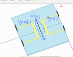
hello everyone, GND vias are usually arranged in a row to isolate signals from both sides as shown in the figure below. I'm curious how to access the isolation effects. there are many papers that draw the EM fields with and without the isolation vias but still not analyzed in quantity. Is there any better ways? thanks for your response.
 

Attachments

  • vias_isolate.gif
    vias_isolate.gif
    226 KB · Views: 139

there are many papers that draw the EM fields with and without the isolation vias but still not analyzed in quantity.
Not sure what your problem is. You can "access" the effect with an EM simulation, which is of course fully quantitative. Or derive simplified models that describe relevant parts of the problem. E.g. model the capacitive coupling by microstrip structures, with or without ground fence in the middle. There are useful approximations for parallel microstrp traces that can be applied in this case.
 
Yes, this is an easy task for EM simulation to calculate the coupling with via fence.
 
Not sure what your problem is. You can "access" the effect with an EM simulation, which is of course fully quantitative. Or derive simplified models that describe relevant parts of the problem. E.g. model the capacitive coupling by microstrip structures, with or without ground fence in the middle. There are useful approximations for parallel microstrp traces that can be applied in this case.

many thanks,FvM. As you said, I want to model the coupling and derive the coupling coefficient. Could you please tell me one approximation analysis, not limited to parallel line? thank you again

- - - Updated - - -

Yes, this is an easy task for EM simulation to calculate the coupling with via fence.

thank you very much, volker@muehlhaus. If use EM simulation, the s parameters can be easily obtained. what about the coupling coefficient? how to simulate to get it?
 

If use EM simulation, the s parameters can be easily obtained. what about the coupling coefficient? how to simulate to get it?

You seem to misunderstand RF concepts. Coupling coefficient is a low frequency concept for inductors. The coupling of lines is more complex than that, it has both inductive and capacitive coupling.

S-parameters for coupling between the lines are easily obtained from EM simulation. This is what we need for RF use. If line 1 has ports 1 and 2, and line 2 has ports 3 and 4, you want to look at S31 and S41.

You can also derive an equivalent circuit model k factor from , but that has a meaning only at low frequency where you can treat this layout as simple coupled inductors.
 
Status
Not open for further replies.

Part and Inventory Search

Welcome to EDABoard.com

Sponsor

Back
Top