savulescucostin
Newbie level 3
Hello everybody,
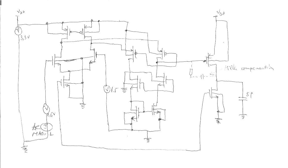
I am asking you for some help with the understanding and designing a diferential operational amplifier with 2 amplifying stages. The first stage must be diferential and use nMOS transistors and the differential stage must use a folded cascode. I actually designed the circuit with some help from someone and I have attached it, but I need to fully understand it and answer questions about it. The circuit must also fulfil the following specifications:
-first stage: differential with nMOS transistors
-differential stage load must be of folded cascode type
-amplification must be 90dB
-band B must be 30MHz
-Miller compensation for stability must be with 60 degree phase reserve
-PSRR more than 80 dB
-capacity(load) used must be C=5pF
-maximum 3.3V power supply

So if someone could please describe in detail the circuit that I have uploaded, where is the Input and Output, what is the use of all the stages, how does the circuit actually work and how do I fulfil all the specifications.
I thank you in advance, all the best!
I am asking you for some help with the understanding and designing a diferential operational amplifier with 2 amplifying stages. The first stage must be diferential and use nMOS transistors and the differential stage must use a folded cascode. I actually designed the circuit with some help from someone and I have attached it, but I need to fully understand it and answer questions about it. The circuit must also fulfil the following specifications:
-first stage: differential with nMOS transistors
-differential stage load must be of folded cascode type
-amplification must be 90dB
-band B must be 30MHz
-Miller compensation for stability must be with 60 degree phase reserve
-PSRR more than 80 dB
-capacity(load) used must be C=5pF
-maximum 3.3V power supply
So if someone could please describe in detail the circuit that I have uploaded, where is the Input and Output, what is the use of all the stages, how does the circuit actually work and how do I fulfil all the specifications.
I thank you in advance, all the best!