hummusdude
Newbie
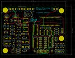
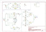
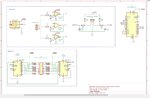
This is an audio pre-amp with a 2 band EQ circuit I found online. There are several digital controls for the gain that are surely overkill but I'm just having fun with different things. The main control is a dpot that controls the gain of the TL072 op amp. The board is 2-sided and the whole bottom is a ground plane.
It's powered by two sources... +- 25 VDC from the main power supply that feeds a couple of linear voltage regulators that supply the 2 TL072 op amps (pre-amp and summing amp), and a 5 VDC source to power the digital components. The design originally used a 5 VDC linear voltage regulator fed by the analog voltage supply but in bread boarding it I noticed it was running quite hot. So I opted instead to use a tiny wall wart SMPS to power the digital components.
This is my first board and I'd appreciate some input about a few things. I'm sure it could be done with a more elegant layout but I'm mostly interested in addressing noise and any other glaring problems that it might have. So my questions are:
1) Is there enough distance between the analog side on the left and the digital side on the right? Aside from the 4 analog signal lines that go to and from the dpot, the closest gap is around 6 mm. Because it uses a dpot I don't see any way to completely isolate all of the analog signal lines. I've read numerous sources about grounding and I'm a little confused on how to prioritize the placing of analog/digital lines.
One source says separate them by at least 20x the thickness of the board, which according to KiCad is 1.6 mm. If that's correct than that would mean it needs 3.2 cm spacing. I can make the board bigger if that is the best option. But that seems a bit out there. And what does that mean about dealing with analog signal lines that have to connect to the dpot?
Another says that the current return path of high frequency lines (>1 MHz) will tend to follow the digital signal lines whereas low frequency signal return paths tend to spread out and also go more directly to the ground connection point. I put the 5 VDC ground point for the digital components far away from the analog ground. The Arduino runs at 16 MHz so that seemed prudent.
The circuit was pretty quiet on the bread board except for some 60 Hz hum which seems normal for the conditions. But I'm worried now that packing it all in so close on a PCB will lead to unwanted noise.
I appreciate any input/advice about my layout or my circuit!