abc_de
Full Member level 5

- Joined
- Jan 9, 2014
- Messages
- 243
- Helped
- 11
- Reputation
- 22
- Reaction score
- 11
- Trophy points
- 1,298
- Location
- Ludhiana ਪੰਜਾਬ
- Activity points
- 2,939
hello
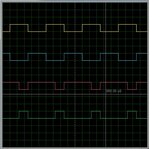
i am working on pwer control pwm of pic18f4431 and try get variable duty cycle of PWM
at 20 khz on all pwm pins. all pwm channels are configure in complementary mde.
i am facing problem while changing duty cycle, frequency of pwm signal is perfect. please help me:???::???:
here is my code
i am working on pwer control pwm of pic18f4431 and try get variable duty cycle of PWM
at 20 khz on all pwm pins. all pwm channels are configure in complementary mde.
i am facing problem while changing duty cycle, frequency of pwm signal is perfect. please help me:???::???:
here is my code
Code:
#include"p18f4431.h"


#pragma config OSC 		= IRCIO	// 	INTERNAL OSCILLATOR IS ON
#pragma config DEBUG	= OFF   // 	DEBUGGER IS OFF
#pragma config LVP  	= OFF   //	Low-voltage ICSP disabled
#pragma config PWRTEN 	= OFF	// 	PWRTEN Disabled
#pragma config WDTEN 	= OFF	//	WDT disabled
#pragma config MCLRE	= ON	//	MCLR Pin Enabled
#pragma config BOREN 	= OFF	//	Brown-out Reset disabled

#pragma config PWMPIN	= OFF	//	PWM outputs disabled upon Reset (default)
#pragma config LPOL 	= HIGH	//	PWM0, 2, 4 and 6 are active-high
#pragma config HPOL 	= HIGH	//	PWM1, 3, 5 and 7 are active-high

#pragma config PWM4MX 	= RB5	//	PWM4 output is multiplexed with RB5
#pragma config FLTAMX 	= RC1	//	FLTA input is multiplexed with RC1

#pragma config SSPMX 	= RC7	//	SCK/SCL clocks and SDA/SDI data are multiplexed with RC5 and RC4, respectively. SDO output is multiplexed with RC7.
#pragma config EXCLKMX 	= RC3	//	TMR0/T5CKI external clock input is multiplexed with RC3

void pwm_int(void);


void pwm_int(void)
{
PORTB=0x00;
TRISBbits.TRISB0=0; //	PWM0
TRISBbits.TRISB1=0; //	PWM1

TRISBbits.TRISB2=0; //	PWM2
TRISBbits.TRISB3=0; //	PWM3

TRISBbits.TRISB5=0; //	PWM4
TRISBbits.TRISB4=0; //	PWM5

TRISDbits.TRISD6=0; //	PWM6
TRISDbits.TRISD7=0; //	PWM7

// interrupt control register
INTCON=0XC0; 		// enabl;e globle and peripheral interrupts
IPR3bits.PTIP=1;	// enable timer 1 interrupt priorty high
PIE3bits.PTIE=1;	// enable timer 1
PIR3bits.PTIF=0;	// disable timer 1 flag


// PWM Special Event Compare Registers
SEVTCMPL=0X00;
SEVTCMPH=0X00;


//DEAD TIME CONTROL REGISTER
DTCON=8; 			// 	dead time arround 2 usec


//FAULT CONFIGURATION REGISTER
FLTCONFIG=0X00; 	// 	disable fault detection feature


//OUTPUT OVERRIDE CONTROL REGISTER
OVDCOND=0XFF;		//	Output on PWM I/O pin is controlled by the value in the Duty Cycle register and the PWM time base.


// OUTPUT STATE REGISTER
OVDCONS=0X00;		//	Output on PWM I/O pin is INACTIVE when the corresponding PWM output override bit is cleared.

// pwm timer register
PTMRL=0X00;			//	PWM Time Base (lower 8 bits)
PTMRH=0X00;			//	PWM Time Base (upper 4 bits)


// PWM TIMER CONTROL REGISTER 0
PTCON0=0X00;		//	1:1 Postscale,Fosc/4 (1:1 prescale),Free Running mode

// PWM TIMER CONTROL REGISTER 1
PTCON1=0X80; 		//	PWM time base is ON


// PWM CONTROL REGISTER 0
PWMCON0=0X50; 		//	All PWM I/O pins enabled for PWM output, complementary mode
// PWM CONTROL REGISTER 1
PWMCON1=0X01;

//PWM Time Base Period Registers
PTPERL=124;			//	PWM Time Base Period (lower 8 bits)
PTPERH0;			//	PWM Time Base Period (upper 4 bits)


//PWM Duty cycle registers
PDC0L=60;			//	PWM Duty Cycle #0L register (Lower 8 bits)
PDC0H=0; 			//	PWM Duty Cycle #0H register (Upper 6 bits)

PDC1L=60;			//	PWM Duty Cycle #1L register (Lower 8 bits)
PDC1H=0;			//	PWM Duty Cycle #2H register (Upper 6 bits)

PDC2L=60;			//	PWM Duty Cycle #2L register (Lower 8 bits)
PDC2H=0;			//	PWM Duty Cycle #2H register (Upper 6 bits)

PDC3L=60;			//	PWM Duty Cycle #3L register (Lower 8 bits)
PDC3H=0;			//	PWM Duty Cycle #3H register (Upper 6 bits)

ADCON0=0x00;// ADC MODULE IS DISABLE


}


void main(void)
{
OSCCON=0X72;   // internal osc. at 8 mhz
ANSEL0=ANSEL1=0X00;  // disable analog pins
pwm_int();
while(1);


}
Last edited:


