Continue to Site

Welcome to EDAboard.com

Welcome to our site! EDAboard.com is an international Electronics Discussion Forum focused on EDA software, circuits, schematics, books, theory, papers, asic, pld, 8051, DSP, Network, RF, Analog Design, PCB, Service Manuals... and a whole lot more! To participate you need to register. Registration is free. Click here to register now.

n and p half bridge fighting

Status
Not open for further replies.

want_to_see

Newbie level 6
Joined
Apr 22, 2012
Messages
13
Helped
0
Reputation
0
Reaction score
0
Trophy points
1,281
Activity points
1,418
hello all,

Im having problem with a half bridge.
The sides seem to be fighting which is generating heat.

The isolated section of circuit causing the problems is a mosfet driver (IDD614) and matched N and P mosfet array (FMP26)
It is being driven from a function generator with 5V peak to peak square wave centered at 2.5V.
Untitled.png

The circuit has been built many times over and I keep having the same problems.
Ive even gone as far as to make a PCB which has teh same problems.


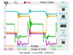
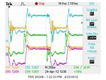
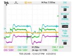
Throughtout the next few images, the same color convention is used where:
yellow: output (pin3 fmp26), blue: p channel gate ( fmp pin 5), pink: n channel gate (fmp pin 1), green: fnction generator input (idd pin 4).

This is the waveform when the circuit is switching 12V
12V_yellowoutput-bluepin5-greenfunctiongen-pinkpin1.jpg

Switching 60V
60V_yellowoutput-bluepin5-greenfunctiongen-pinkpin1.jpg

this is the output with just the function generator on and power supply swtiched off
is it a loading issue? I just dont understand this.
no_power_yellowoutput-bluepin5-greenfunctiongen-pinkpin1.jpg


As the rate of switching speed is increated, the "fighting" takes up a larger percentage of the waveform.
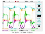
1.1MHZ_60V_yellowoutput-bluepin5-greenfunctiongen-pinkpin1.jpg

When a the load (1nf capacitor) is connected at teh frequency i want to run at, 1.2Mhz,, the loading becomes worse
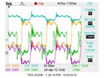
under1nfload__1.2MHZ_60V_yellowoutput-bluepin5-greenfunctiongen-pinkpin1 - Copy.jpg

When I was searching for a solution to this, I came upon this post when i why i registered.
Its somewhat similar but the load here is capacative not inductive.
I realy appreciate any help i can get on this.
https://www.edaboard.com/threads/241410/
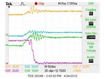
 

Well, first of all, you've got your half-bridge drawn wrong-the upper MOSFET is upside down.

I'm not quite sure how this all works with those caps driving the gate, but I'm suspicious about those 10K resistors. If you are counting on those to turn your devices off, you're in trouble. The MOSFETs have a huge input capacitance (about .003uF); coupled with those 10Ks, that's a time constant of about 30uS.

Also, your function generator input has a serious glitch in, maybe you've got some grounding/power supply issues.
 

barry,
yes, there is big capacitance.
there is only one 10k resistor, the other is 100ohm.
changing the 10k to a smaller value, ie 220ohm does not fix the problem.
there does not appear to be a problem with a time constant, it switches very fast.

I have 3 function generators, and tried them all out, and have identical problems with each.
I also have a drive system made from a 555 which also has the same switching probem.

one thing that is funny is that if i change the supply voltage on the mosfet driver, the fighting appears to get worse over 10V
The function generator is set for 5V peak to peak, and there is a common ground, if this signal amplitude is varied, it also seems to make the mosfets fight more.


thanks for finding the problem with the mosfet in the schematic i drew up.
 

I still don't like those caps on the gate. When you, for example, drive the input to those caps high, the gates will both go high, but the N-channel will then immediately start to decay through the resistor.
I would zoom in on the edges of the two gates, and you'll probably see some overlap there that is causing your problem. You also might want to try a resistive load first. And make sure your mosfet power supply is at LEAST 10 volts, or you won't turn the mosfet completely on.
 

i really appreciate your time barry

the caps are for DC biasing.
the half bridge is configured to switch from 0 to 60V
but i can also switch -60 to +60V .
so the caps help configure independent biasing of each gate in reference to the supply by blocking the DC.


i lowered teh 10k resistance, increasing the DC on the gate with the following.
Untitled.png

this is a zoom in of the switching, this without a load
pink is the output
green function generotor
and yellow and blue are the gates
off.jpg
off.jpg
 

it just dosent work with the ..1u caps removed
i adjustable VDC shows a short.
there is no one way to bias it, or even not, as its all one node
 

I guess there is a good reason why high side MOSFET drivers exist and people don't try to use capacitors to drive MOSFET gates normally. I don't think you have actually said what the objective of your circuit is.

Keith
 

IXDD614 has huge prop delay at low Vdd, Try to run >20V for Td ~ 50 nS
Start at 1KHz and check for operation using a very short ground clip. preferably none with probe tip removed & a coaxial coil to cct bd. or use SMA connectors on board. Your scope signals are messy.

Check capacitance loading effects of zener diodes.
CM ferrite choke to Motor would help too.
 
Last edited:

I guess there is a good reason why high side MOSFET drivers exist and people don't try to use capacitors to drive MOSFET gates normally. I don't think you have actually said what the objective of your circuit is.

Keith
40000 posts, incredible.:shock:
Im on a unrelated BB with 12000, I can appreciate your dedication

sorry, there is a balance with trying to be concise and providing enough information.
In this case, the circuit should be driving an ultrasound transducer, a piezoelectric element which can be modeled as a capacitor.
The load will vary from around 1 to 20nF (depends on area of transducer).
The driving rate would be around 50kHz to 2Mhz.
Of course, the impedance of the ultrasound (1/wc) will change as the frequency changes, so output power will not be constant as the frequency changes with a contant voltage. I can live with this.
The general range of MOSFET drivers from IRF are really only supported to about 500kHz
So I have been trying to come up with some of my own solutions.
Even at 500khZ, most IRF chips produce excessive heat as it is end the top of their range.
One chips that works well for me is the EL7158
It is able to drive currents needed as the large gate capacitance that develop as the higher rates of frequency (ie 1Mhz vs 1kHz)

Anyway, i need something that can run stable for hours on end driving this type of load.
Something that can be easily heat sinked (unlike EL7178), preferably not surface mouth, nor that is prone to latching.

Im not that sure about the exact differences between high and low side drivers and was hoping i could get away with either since there is a high side and low side both in one chip (FMP26) with 5 pins. I know the difference has to do with how they are referenced. But I need to drive the chip with something and dont want to get over complicated such as using a microcontorller. The limitation of most ICs for gate driving is that I have to provide the two independent input signals and Im hoping there really shouldnt have to be anything that complicated for this.

Any ideas.
I do agree something looks funny with the power / referencing as when its increased, a more pronounced ringing occurs and becomes worse.
Its not a biasing issue, no way, no matter what i do, it rings.
 
Last edited:

When you want to drive large signals to complex impedance, with non linear drivers, and harmonics suppression is important, one must start to think about creating a controlled impedance network and determine what the real load characteristics and try to make the generator and transmission line match the load. YOu may have to put a dummy load across the Piezo device to reduce ringing from reflections and feedback as well as increase the source resistance. to match the load. Just a thought. I would start with a complementary common darlington emitter-follower "damn fast buffer" + 50 ohm = driver for large signals to see if that works better. The Piezo will provide many modes of complex poles & zeros in impedance vs f. Can you plot it with scan? or monitor current envelope vs F on an X-Y sweep?

Of course you can reverse engineer what has already been done, like I just did...
1)

This is how the pro's do it and have no ringing and high power to 10 or even 50MHz piezo +/- 100V > 400W.
BUT
Precautions need to be applied to not overlap the logic-high time periods of the control signals. Otherwise, permanent damage to the device may occur when cross-conduction or shoot-through currents exceed the device’s maximum limits.
You can try to emulate these $$$ hybrids with discrete design. Note Diode OR of High side and low side outputs.
 

Attachments

  • datasheet-1.pdf
    122.6 KB · Views: 112
  • datasheet-3.pdf
    852.6 KB · Views: 103
  • datasheet-2.pdf
    102 KB · Views: 97
Last edited:
sunnyskyguy, i saw your posts
Im going to try this stuff tomorrow when im infront of the circuits.

It is impedance matched somewhat
Its very small impedance matching network with this load though.
I did the computations via smith chart and came out with mostly real resistances and the matching would be a series inductance in the 2-3nH.
I had a fellow check it with a network analyzer and he came out iwth 2 uH series inductor neeeded.
Both are just so small, its not really worth trying to do.
If anything, i may need a small series resistor to match it somewhat, ive tried that, it makes the oscillations bigger.
i want to reduce oscillations before i do anymore
Im getting oscillations with no load and chip is getting hot, it just gets worse wtih the load though.
thanks for your time!
 

While I am not very comfortable with the idea of trying to use capacitors to drive MOSFET gates, if we look at the reasons why it may have problems, maybe they can be solved for your application.

I would suggest simulation is a quicker way to explore new designs if you have it. If not, LTSPICE would be worth considering (it's free). You can try out lots of ideas quickly without buying components, building things and blowing them up. Also, you can probe certain things a lot more easily such as gate current and you can actually measure power in devices rather than waiting for them to warm up and guessing at the power. You can also separate the NMOS from PMOS dissipation which is difficult in a single package with actual devices.

As already mentioned, you seem to have some problems with the probes you are using. The ringing is on all waveforms (including the signal generator) so cannot be considered to be real. An easy check is to probe the point you have your ground clip connected to. You should get nothing. If it is ringing then it is being picked up in the ground wire.

I don't know the SRF and ESR of your capacitors but I would think something smaller in parallel (e.g. 1nF) may be required.

Driving the gates with a capacitor with a long time constant (relative to the clock rate) means the gate voltage will settle at +/-5V when driven with 0V/10V. So, as well as driving the gate negative (for the NMOS) you have lost half your drive voltage. This will obviously affect your ON resistance.

In my experience excess power dissipation often comes from slow switching rather than the devices clashing. This is not to say that you don't have clashing drivers, but if the transition times are short the lost power can be small. This comes down to fast, high current gate drivers.

It would be worthwhile looking at the IXD614 output as well as the input. Any effect (such as charge storage or reverse transfer capacitance effects) from one transistor could be affecting the gate drive of the other transistor. Using two IXD614 chips rather than one may help.

A better model for the piezo is a tuned circuit. As you have a network analyser you should be able to create your own model.

I have seen people try to reduce or null the parallel capacitance in piezos so they are just driving the series tuned circuit (which should look resistive at resonance) but it is not something I have ever found much success with. The inductance required always seem to cause more problems than it solves.

You are flattering me with the number of posts - I think you have looked at the number of points. Even FvM has only managed 16000 posts :shock:

Keith.
 
keith, thanks
i think there is a simuliation model for cadence that is free.
i usually just use that.
but there are no models for the chips in use
have to really have very mathced switching speedings for it to be of any value as it is very high precision.

i know about how the reference makes the signal look different.
thanks for pointing that out though, it is a key issue that can be missed.
this is not that though.

ok, well, we just decided to ue the circuit as is.
just very large heatsinks on it.
im really not sure what is normal and what is not in terms of heat dissipation.
There is not enough of a detailed spec sheet for this device, fmp26, to really know and thats the problem.
really should have just made my own.

ok, thanks everyone
 

Hi

I don't have a problem, in principle, with the way the gates are being driven, but I am concerned about a few details:
The circuit has been built many times over and I keep having the same problems.
Ive even gone as far as to make a PCB which has teh same problems.
This is a little worrying as it suggests that physical layout is not being taken seriously enough, and a PCB is considered optional. For high speed switching like this, the layout is very important as, for example, wiring inductance can be significant, and will cause (or affect) ringing on the waveforms. Some of your pictures do show a significant difference between the waveforms at the gates of the two MOSFETs.

I also don't understand why the two resistors are so different in value. first you used 10K and 100 Ohms, then changed to 220 Ohms and 10 Ohms. Is there any good reason why these should not be similar or the same e.g. both 100 Ohms?

Another possible problem is the different switching times of the N and P channel devices.

It may be worth deliberately slowing down the rise and fall times of the input square wave, to make sure one device switches off before the other switches on. This could be done by putting a small resistor between the driver chip and the coupling caps, which would also help damp the ringing.

Perhaps the biggest problem is that you are driving a capacitive load. This is very different to driving a resistive load.

Firstly, the voltage across a capacitive load cannot be changed instantaneously, and attempting to do so (with a square wave) will result in very high peak currents through the MOSFETs. This is another reason to slow down the rise and fall times, as it will reduce the peak currents.

Secondly, and more importantly, The MOSFETs have to dissipate a certain amount of energy in order to charge or discharge the load capacitance. That means that even if there is no cross-conduction (fighting) between the MOSFETs, they will be dissipating a significant amount of power, and that power will be proportional to the switching frequency.

There is no easy way around this. One option is to put a small resistor between the output and the load. That will reduce the power dissipated by the MOSFETs, but that power will now be dissipated in the resistor. Total power dissipation will be the same. An output inductor could solve this problem, but would be difficult to specify if operating frequency and load capacitance are both variable.

Regards - Godfrey

(just my 2c worth)
 

the solution turned out being to increase the resistance between the mosfet driver and mosfet... the lower impedance worked at lower voltage but now the high voltage
 

Examine the currents and effective series resistance of the gate and the Cap load. Dont expect good results if you are expecting a gain more than 100x ie. the load ESR of the Cap+ FET is 100x less than the ESR of the source driver
 

Status
Not open for further replies.

Part and Inventory Search

Welcome to EDABoard.com

Sponsor

Back
Top