Continue to Site

Welcome to EDAboard.com

Welcome to our site! EDAboard.com is an international Electronics Discussion Forum focused on EDA software, circuits, schematics, books, theory, papers, asic, pld, 8051, DSP, Network, RF, Analog Design, PCB, Service Manuals... and a whole lot more! To participate you need to register. Registration is free. Click here to register now.

Multiple Grounds issues in Cadence LVS

Status
Not open for further replies.

Ali263

Member level 1
Joined
Aug 21, 2020
Messages
40
Helped
0
Reputation
0
Reaction score
1
Trophy points
6
Activity points
450
Hi ,

I am designing a circuit in 65nm cmos process which has different VSS connections for analog and digital part(VSS! and AVSS).

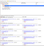
However whatever i do, i get the below 50, 50 errors as shown in picture attached.

Can someone understand from the attachment what exactly it means?
What is the meaning of two **VSS! or **AVSS?
 

Attachments

  • lvs.PNG
    lvs.PNG
    118.5 KB · Views: 153

It's clear what it means - you have one net, AVSS, in the schematic (source), but two nets in the layout - AVSS and VSS!

Somehow, the bulk of the MOSFETs gets connected to VSS! - that why there is instance (pin) mismatch between schematic and layout.

I do not know how to resolve this, but this should be a pretty standard situation, and the resolution should be easy and well known.

You can try declaring AVSS net as a ground - the instance mismatches should go away (but net mismatch will still be there).
 
Many PDKs have inherited connections that default to a "safe" global net like vss! If the net property is not set explicitly or by wire with the B terminal exposed. Check properties for stale VDD! references.
 

Status
Not open for further replies.

Part and Inventory Search

Welcome to EDABoard.com

Sponsor

Back
Top