majun
Newbie level 1

Hi,
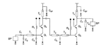
I am new for the IBM SiGe BiCMOS 0.13um Process.
There are bondpad and bondpad_inh in the Schmatic,but no pad. There are bondpad and pad in Layout.
When I simulate the Schematic, should I put in a bondpad in my design? Or after layout design put in a pad in the layout.
and it is right and necessary to put a simulation term after the bondpad I/O?
Attachments
Last edited: