Continue to Site

Welcome to EDAboard.com

Welcome to our site! EDAboard.com is an international Electronics Discussion Forum focused on EDA software, circuits, schematics, books, theory, papers, asic, pld, 8051, DSP, Network, RF, Analog Design, PCB, Service Manuals... and a whole lot more! To participate you need to register. Registration is free. Click here to register now.

[Moved]Single side PCB routing

Status
Not open for further replies.

Mayank_rob

Newbie level 2
Joined
Jan 18, 2015
Messages
2
Helped
0
Reputation
0
Reaction score
0
Trophy points
1
Activity points
22
Hi there,
I am trying my hands on making PCB files myself. I am making PCB in my college so i am very limited with tools available. I can make only one sided PCB, i use corrosive etching to remove the unwanted copper lines.
I have done some trial and error myself, using help of few websites.
But now i was looking some reviews and comments to improve my board.
I wanted to reduce the unrouted paths as much as possible.
Any suggestion would be of great help.
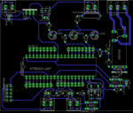
I am attching snapshot of schematic and board layout.

thank you

Info:-
software:- Eagle
Project:- Intrusion detection using Reed sensor & 89s52.
 

Attachments

  • board.png
    board.png
    115.8 KB · Views: 82
  • schematic.png
    211.1 KB · Views: 77

Re: Single side PCB routing

It's quite normal to provide a number of umper wires with single sided PCBs. You'll find it also in home appliances with simple control boards.

To minimize the number of jumper wires, you would partly rearange component placement.
 

Re: Single side PCB routing

If you have a layout program that provide a "rats next" view of the wiring that will help see which placement and orientation of the parts leads to the fewest crossovers.

If you don't have that, then just look at where the wires go between the parts and arrange the part locations and rotation for fewest crossovers. That can take some time to get the optimum arrangement. Also note that you can run traces underneath parts, even surface mount types, (as long as the minimum trace width and spacing rules are followed).

Note that the neatest looking layout or orientation may not be the optimum for minimizing crossovers.
 

Re: Single side PCB routing

OK. I have pretty much thought about it. And this is my third board, after trial and error so i think i will stick to it and will use jumpers and wires to connect it.
I just had 1 more question:-
When i use polygon to fill the unused areas, the clearance between the tracks and ground layer is very less. i mean the track and the ground layer gets shorted because etching method is not very efficient method of making PCB. So how can i increase the distance between track and ground plane...i tried changing number of parameters but none seem to help/
 

Are you able to swap the positions of the supply & sensor terminal blocks?

Might make the layout of the higher voltage side easier as it's close to the relay it also connects to.

If staying as they are then swap the supply terminal block pins & it will layout much better in that corner.

What voltage will be on the relay? you have a nice distance for the NC track but the COM pad is very close to it, can you change the pads to be 90 degree rotated on that relay? (or plain round pads).

For the copper polygon - read this:
http://dangerousprototypes.com/2012/07/18/eagle-polygons/
 
Last edited:

You have a number of acid traps in your layout. You might want to address them as they could affect reliability if the board isn't thoroughly cleaned.

Here are a few examples:
Capture.JPGCapture2.JPGCapture3.JPG

Anywhere you have less than 90 degree intersections are problematic.
 

Status
Not open for further replies.

Part and Inventory Search

Welcome to EDABoard.com

Sponsor

Back
Top