Continue to Site

Welcome to EDAboard.com

Welcome to our site! EDAboard.com is an international Electronics Discussion Forum focused on EDA software, circuits, schematics, books, theory, papers, asic, pld, 8051, DSP, Network, RF, Analog Design, PCB, Service Manuals... and a whole lot more! To participate you need to register. Registration is free. Click here to register now.

[MOVED]Problem dealing with 4 layers in Eagle

Status
Not open for further replies.

Ricewind

Newbie level 6
Joined
Mar 14, 2011
Messages
13
Helped
0
Reputation
0
Reaction score
0
Trophy points
1,281
Activity points
1,412
I have recently moved to design a 4-layer PCB due to the needs of the project I am doing.

The thing is that I get a little problem when I want to do some planes for the ground and supply signals in the inner layers. When I do the polygon and click the ratsnest button, the copper covers all the inner area, without avoiding the vias which do not route signals to that precise layer.

It only avoids those vias in case I have a routing line in the same layer which is not included in the signal of the polygon.

Can anybody help me how to do this right? in this precise moment, Eagle will shortcut all my vias :-/

Thank you in advance
 

Re: Problem dealing with 4 layers in Eagle

You are saying that the plane shorts vias? You may have to upload the file so we can take a look. If you highlight the net by clicking on one of the vias after selecting "Show", does it highlight all the other vias and the polygon?

Keith.
 
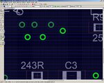
viasdelcaos.jpg

That´s it, the plane shorts all the vias... i do not know really why is this. I opened a new project and did some proofs and they are alright.

The only difference I see is that, at placing vias, it appears this coloured circle within the vias (blue in the image).

When selecting "show", I see the correct vias highlighted with the polygon. Those which should not be highlighted are not, but anyway they are shortcut!

I have seen that eagle does not shortcut the vias if there is a specific signal (wired, I mean) between two vias in that plane.

I am sorry I cannot upload the complete project, but I hope the image capture will help to see what I mean.

Thank you very much for your time
 

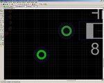
viasdelcaos2.jpg

no doubt, at selecting "show" only the right vias are highlighted with the polygon
 

I cannot say that it is shorted. Maybe you should try using different colours for the different layers - I think you have two layers which are blue so it is impossible to tell what is what. If you upload the Eagle file it would be easier to check.

Keith.

---------- Post added at 09:26 ---------- Previous post was at 09:25 ----------

By the way, if you prefer, you could send me the file by private message.

Keith.
 
I copy here the answer given to me by keith1200rs, if it can help anyone further

You have drawn a polygon connected to a net and ALSO defined it as a power plane. You should do one or the other - not both. I will try to explain:

Power planes are negative layers. Normally you would not draw anything on that layer at all. When you define it as a power plane layer and give the layer of the net, it will automatically connect to that net, but as it is a negative layer, what you will see is where it ISN'T connected.

With a polygon fill, you draw the polygon, name it as the net you require and it will connect. That tends to be the better way of doing it really. You will see unconnected nets easier, if there are any, and it is easier to do cuts and special shapes.

In your case you have defined it as a plane layer but the name is ROUTE2 or ROUTE3, not GND. You have also drawn the polygon. Simply unclick the box on the two inner layers "Supply Layer" and your problems will be solved.
 

Had anyone tried gerber file for 4 layer printboard... coz m nt able to generate those inner layers properly... plz help me out...:sad:
 

You need to use a CAM file which is intended for 4 layers. The default installation should include one called gerb274x-4layer.cam - use that.

Keith.
 

I did tried that as well bt no use.. i dont have much knowledge of eagle and electronics .. inner layers are not proper..
 

What do you mean by "inner layers are not proper"? You need to show your layout and the Gerber files you produced for someone to help.

How have you created your inner layer? Are they polygon fills or did you click the box to make the power plane layers? Plane layers which are not created with polygons will be negative layers. The PCB processing will turn them in to positive images. I would recommend you use polygons for power planes anyway - the DRC and electrical connectivity checking is better.

Keith.
 

Can i mail that to u... pls u jst have a look and correct me...
 

see this attachment..
 

Attachments

  • printrboard.rar
    136.9 KB · Views: 88

Any idea about 'FIDUCIAL1X2.5"...?
 

Detailed information of this component..
 

I am not sure which library that is in (and hence don't know the exact shape) but fiducials are for marking the PCB for helping the PCB pick & place equipment. They can be global i.e. for the whole board, or local, near a specific component. Search the forum for FIDUCIAL in the title to get various discussions on what and where to place them.


Keith.
 

Any idea about "SJ_2S" and "SJ_3 Connected".. what are they..??
 

They sound like solder jumpers to me - used to make optional connections on the PCB with a solder blob. Which library are they in? Have you looked at the "description" in the library - that usually gives a good clue e.g. SJ has the description "SMD solder jumper".

Keith.
 

Would Like to know the detail difference between Optical switch and Mechanical switch .??
 

Status
Not open for further replies.

Part and Inventory Search

Welcome to EDABoard.com

Sponsor

Back
Top