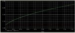
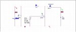
Continue to Site

Welcome to EDAboard.com

Welcome to our site! EDAboard.com is an international Electronics Discussion Forum focused on EDA software, circuits, schematics, books, theory, papers, asic, pld, 8051, DSP, Network, RF, Analog Design, PCB, Service Manuals... and a whole lot more! To participate you need to register. Registration is free. Click here to register now.

[Moved] orcad simulation problem boost circuit

Status
Not open for further replies.
Re: orcad simulation problem boost circuit

Do you expect a MOSFET being turned on with 1V gate voltage? Show the gate waveform.
 

You are using a digital stimulation signal instead of an analog pulse generator to drive the MOSFET, apparently without understanding the specific behaviour of the mixed signal (PSpice AD) tools.

Two options:
- read the AD user manual to learn how to use the mixed signal features correctly
- use a regular VPULSE source
 
Thanks FvM , for providing usefull information

my output is rising too slow and I want to make it constant at 6V . How can i do that?
 

Attachments

  • 1.JPG
    1.JPG
    84.2 KB · Views: 119
  • 2.JPG
    2.JPG
    45.2 KB · Views: 123

Constant duty cycle will never give constant voltage, you'll use a PWM controller utilizing a voltage control loop.
 

How can I do that , is their any provision in orcad for it.
 

Use a PWM controller IC model, or more instructive, design a simple behavioral model of a PWM controller comprised of a reference voltage, an error amplifier with PI characteristic, a triangle voltage source and a comparator.
 

Hello FvM , I am looking for logic level MOSFET in orcad simulation
 

which PWM controller IC should i use
 

Hello FvM , In circuit my both MOSFET M50 and M51 gate connected at different voltage, but both capacitors C1 and C2 getting discharge with same rate
 

Attachments

  • 10.pdf
    8.6 KB · Views: 103
  • SCHEMATIC1 _ PAGE1.pdf
    12 KB · Views: 97

This simple boost converter simulation resembles one of your schematics.

It uses a transistor switch instead of a mosfet.


The waveforms are typical in a boost converter.
 
Thanks bradtherad, Can i do IC level layout of this boot converter in orcad
 

Thanks bradtherad, Can i do IC level layout of this boot converter in orcad

The inductor needs to contain a certain amount of ferrous metal to work.

So if you are asking whether an entire boost converter will fit on an IC, then I believe the answer is no.
 

Ok , after leaving inductor can i fit other component on IC
 

The load capacitor is also too large to put in an IC.

I suppose you plan to add the control circuit? The control circuit needs to be smart. It must manage two behaviors. It must maintain on-off action in the transistor. It cannot allow it to stay on.

The control circuit must also monitor output voltage. It must alter the duty cycle, so that it maintains your desired output voltage.
 

Ok I just want to do layout of that transistor or MOSFET, know this is possible. Can you tell me, how can I do that in orcad?
 

Status
Not open for further replies.

Similar threads

Part and Inventory Search

Welcome to EDABoard.com

Sponsor

Back
Top