nisha gupta
Member level 4
- Joined
- May 22, 2012
- Messages
- 71
- Helped
- 0
- Reputation
- 0
- Reaction score
- 0
- Trophy points
- 1,286
- Location
- Hyderabad, Andhra Pradesh, India
- Activity points
- 1,755
hi
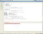
i have simply design a inverter in 65nm and completed layout so that i can understand all layout process in 65nm. i have cleared DRC in LVS i have given the path of rules file. and for inputs i have given file path but i not able to give correct path for layout netlist so it is giving some error. i m attaching the sreenshot of error message. kindly help me out .
i have simply design a inverter in 65nm and completed layout so that i can understand all layout process in 65nm. i have cleared DRC in LVS i have given the path of rules file. and for inputs i have given file path but i not able to give correct path for layout netlist so it is giving some error. i m attaching the sreenshot of error message. kindly help me out .