Continue to Site

Welcome to EDAboard.com

Welcome to our site! EDAboard.com is an international Electronics Discussion Forum focused on EDA software, circuits, schematics, books, theory, papers, asic, pld, 8051, DSP, Network, RF, Analog Design, PCB, Service Manuals... and a whole lot more! To participate you need to register. Registration is free. Click here to register now.

[SOLVED] [MOVED]How to fix the receiver unit of this radio?

Status
Not open for further replies.

yo2550

Member level 2
Joined
Nov 26, 2011
Messages
44
Helped
0
Reputation
0
Reaction score
0
Trophy points
1,286
Activity points
1,675
**broken link removed**

**broken link removed**

**broken link removed**

**broken link removed**

**broken link removed**

**broken link removed**

**broken link removed**

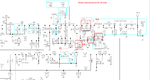
The receiver circuit should have been distorted after I tested the radio with my DIY power amplifier. Once, the ANT was shorted to 12v. power from a battery. The problem may also come from testing the radio with the PA many times with a high SWA.

This results in less sensitivity of signal receiving comparing to another same model of the radio. I tried adjusting the RV1, which is supposed to be a squelch but the problem still exists. I cannot receive weak signal while another same model one can. This radio is auto squelch, there is no SQ dial.

So, I'm thinking of changing the Q6, Q8, Q9 but I'm not sure if it would fix the problem.

Please tell me which components should I change to fix the receiver unit of this radio.

The Schematic Diagram is in the TH7_X7A.pdf file.

Thanks.
 

If you do not know this specific model, please tell me if it is right to replace the first or second transistors in the receiver circuit when it has a problem?
 

Anyone wanna help me with this issue? I'm waiting for your kind contribution.
 

Supplementary ( to the idea of replacing Q6, Q8, Q9) search the receive path for bad solder joints and cracks in the PCB area.
You need to consider also the TX/RX switching diodes(D13, D1, D8) may be the cause for low sensitivity so need to be checked , and C7 / C39 / C179 low capacity can cause poor reception operation also. Those capacitors can be easily tested in circuit. You can put one small ceramic capacitors in parallel and their values will add up.
Check Q26 transistor voltages : base = 0V , collector = 6V (voltages to be measured in the RX mode) .
 

Attachments

  • Receiver amplif.png
    Receiver amplif.png
    115.6 KB · Views: 215
  • Like
Reactions: yo2550

    yo2550

    Points: 2
    Helpful Answer Positive Rating
I checked Q26 collector voltage is the same as battery voltage, but the base voltage is around 0.05 volts. I don't know if this is normal.

R10, R11 voltages are the same as battery's.

D13, D7 voltages are not 0 but around 5.6 volts. I think this is the problem.

Any advice please?
 

Once, the ANT was shorted to 12v. power from a battery.

Looking at the schematic. (I see an antenna input at the upper right, but what do I know?). See if you can locate a component that could have its operating characteristics changed by a sudden DC jolt. It might cause lower sensitivity in the detector stage.

Are any of the diodes near the antenna of the small signal type that would be harmed by a jolt? Are any capacitors near the antenna rated less than 12V? Probably none are electrolytics? A jolt of wrong polarity could ruin an electrolytic.

Does the receiver section have a sensitivity rating? 1 uV perhaps? Can you apply a 1uV carrier signal to the antenna input? Through a high impedance so you can determine whether a lower impedance somewhere drains it to ground (example, a faulty capacitor)? See if it reaches the amplifying stages?
 
  • Like
Reactions: yo2550

    yo2550

    Points: 2
    Helpful Answer Positive Rating
Thanks. Could you tell me if I can check the transistors and capacitors on the board without removing it? Ex. C7, C39, C179
D1, D8, D7, D13 is working as I tested them with multimeter.
The point at the right of D13, D7 show DC5.7 volts. Is this voltage leak?
 
Last edited:

Only a few components can be tested in circuit. Usually you must disconnect all but one leg of the device you are testing, or else any readings are liable to include neighboring components.

Alert: Find out how much current your ohmmeter puts out, especially on the low range. For instance my analog meter produces 60 mA at 1.5V, which could fry delicate components. I believe a DMM puts out much less current.

D7 and D13 appear to receive DC by way of L8, from what I can see. It goes to a wire labelled B1 (I suppose that has 6V). I think it is normal for 5 V to appear at their right.

The transistors customarily have the bias at a volt level 0.6 different from the emitter. So Q26 may be faulty if it shows .05V.

Caveat: I don't know how this particular radio circuitry works, and I'm confused at seeing many transistors are oriented to function as a transmitter. However I also see a mic at lower left. Is it a transceiver?

Does the transmitter function okay? If not then you are probably looking for a component that is common to both functions, and may be diverting incoming signal somehow, reducing receiver sensitivity.
 
  • Like
Reactions: yo2550

    yo2550

    Points: 2
    Helpful Answer Positive Rating
Thanks. Talking about Q26, I checked the voltage by touching the red lead at the collector leg and black at the - of battery in RX mode. mister_rf told me the base voltage should be 0V., and collector voltage should be 6V.
The radio is the 4.5Watts transceiver as you can see in the pdf files.
The transmitter function is working ok from what I noticed.
I will check Q26 again and tell you the voltage of collector to emitter.

- - - Updated - - -

Ok I checked the Q26, the collector to emitter voltage is 6.6V. in RX mode and 0.15V.-0.24V. in TX mode. For Base to GND in RX mode = 0.02V. The same as Emitter to GND = 0.02V.
Is this normal volatages of the Q26?

Update: I check the Q26 of another same model good radio and the Base to GND shows 0.02V. too. So I believe that the Q26 on my radio is working.
So, which parts should I check then?
 
Last edited:

It appears that Q26 is working okay. I guess its purpose is to turn off during receiving, in order to isolate the circuitry used for transmitting. Since battery V appears across C-E during reception, then it is going high impedance.

From post #1:

The problem may also come from testing the radio with the PA many times with a high SWA.

Does SWA have to do with standing waves in the antenna wire? I am not expert in radio and antenna operation, but this sounds like it could mean a strong AC signal was going into the receiver front end. This could get through capacitors, perhaps with greater possibility to damage components.

The incoming rf signal is either getting choked, or diverted, or not being amplified sufficiently.

I think (though I don't know) that Q6 is the first amplifying stage. It may be necessary for you to disconnect a few components, in order to make sure no incoming signal is diverted away from the amplifier stages. Particularly between L3 and D7-D13. And to the right of D1. (If you can get to these.)

When clipping leads, avoid doing it quickly because a sudden mechanical shock can carry into the component and damage junctions.
 
  • Like
Reactions: yo2550

    yo2550

    Points: 2
    Helpful Answer Positive Rating
Yes, it is SWR. I typed it incorrectly.

I think you understand it correctly about Q26 as I read from TECHNICAL DESCRIPTION in the pdf file. Here is the content of the file.

"
TECHNICAL DESCRIPTION
Page 1
A). GENERAL DESCRIPTION
The TH7 radio is a self-contained transceiver unit with integral antenna
intended for use as a general communication tool. It is designed to operate
on all 80 channels. This model also features user selectable sub-audible
tones for channel quieting. The useable range, while dependent upon terrain
and other radio propagation principles, is typically 8 miles. The TH7 uses the
maximum transmit power allowed to help ensure the maximum
communication range.
Features include: 80 Channels, Channel Monitor, Page and LCD Display.
The unit is equipped with an external Headset option connector. Four AA
alkaline batteries that are readily available in retail outlets supply operating
power. An automatic power savings feature allows the typical standby battery
life to extend to more than 3 days.
B). FREQUENCY DETERMINING CIRCUITS
The fundamental frequency for both the transmitter and the receiver
local oscillators are controlled by a phase lock loop (PLL) circuit IC201
(Toshiba TB31202, or equipvalent). The frequency of operation of the FRS
voltage controlled oscillator (VCO), composed of Q301 and Q302 operating in
cascade is phase locked to a voltage controlled crystal reference (VCXO)
operating at 20.95MHz (X202).
The VCO is locked to the fundamental of the transmit signal in the transmit
mode and is locked to the receive 1
st
LO (Fundamental channel frequency
minus 21.4MHz) in the receive mode. The crystal reference frequency is
shared with the 2
nd
LO of 20.95MHz.
C). TRANSMITTER CIRCUITS
The transmitter amplifies the 0 dBm signal from the VCO to
approximately 27dBm that is fed to the antenna. The transmitter is a three
stage amplifier composed of Q1,3,4 and Q11. The first two stages are
operated class A and the final is operated class B in full saturation to help
prevent unwanted amplitude modulation. The fundamental transmit signal is
fed through an elliptical low pass filter (5-pole, 2 zero) in order to suppress the
harmonics to below –50 dBc. The desired frequency modulation of the carrier
is accomplished by modulating the current in the VCO directly with the
microphone audio signal. The microphone audio is conditioned with a threepole high pass filter at 300 Hz (IC5C,D), a hard clipper circuit (IC5B) to limit
maximum deviation to +/- 2.5 kHz and a three-pole low pass or splatter filter at TH7
TECHNICAL DESCRIPTION
Page 2
2.8 kHz (IC5A). The low pass filter insures that the occupied bandwidth of the
FM modulated signal meets Thai requirements under all input conditions.
D). RECEIVER CIRCUITS
The received signal from the antenna is band limited to 300Mhz by the
transmitter harmonic filter. The desired signal is fed to a low noise amplifier
(LNA – Q6) centered from 240 to 250 MHz that provides approximately 10 dB
of gain. The output of the LNA is filtered with a Band Pass filter (SF1) with
pass-band of 242 to 247MHz and stopband attenuation of 50 dB. The filtered
receive signal is one input to the 1
st
mixer (Q8), the other mixer input (1
st
LO)
is the output of the VCO at the desired channel frequency minus 21.4MHz.
The output of the mixer is tuned to the 1
st
IF of 21.4 MHz.
The 1
st
IF is transformer coupled for impedance matching to a X-tal filter
centered at 21.4MHz with a bandwidth of +/-3.75Hz. The filtered 1
st
IF is then
amplified by Q9 and fed to the 2
nd
mixer input of the multi-function receiver IC
(IC1). The 2
nd
LO (20.95 MHz) is generated by VCXO that is the reference
frequency for the PLL. The 2
nd
mixer output of 450 kHz is filtered through a 4
section ceramic filter that in combination with the 21.4MHz X-tal filter provides
approximately 50 dB of adjacent channel attenuation. The 450 kHz 2
nd
IF is
then amplified, limited and fed to a quadrature detector for FM demodulation.
The resulting audio output signal is bandpass filtered from 300 to 3 kHz (Q22)
and amplified to provide 150mW of audio power (IC2). A squelch circuit is
provided (IC1 pins 10 through 11) to mute the receiver noise under low signal
conditions. The squelch circuit amplifies and detects noise in a narrow
bandwidth at approximately 5 kHz. When the detected noise exceeds a
threshold set to trigger at approximately 9 dB SINAD receive signal strength,
the audio output is muted.
E). TRANSMIT/RECEIVE SWITCH
When the radio is in the transmit mode, pin diode switches D13 and D1
are both turned on (representing less than 0.7 ohms). D13 allows the transmit
signal to pass to the antenna and D1 shorts one leg of a T matching network
(L3, L15 and C4) to ground in the receive path. This results in a parallel tuned
circuit high impedance being presented to the transmit signal so that the
receive path does not load the transmit signal. In the receive mode, both D13
and D1 are off, resulting in the antenna signal being coupled into the receive
LNA through the 50 ohm T matching network and the unwanted load of the
transmit final amplifier is reduced to less than 1 pF by D1.

F). RADIO CONTROL CIRCUIT
A microprocessor (CPU1) is used to control the transceiver. User stimuli is
provided through a tack switch for PTT (push to talk), along with the keypad
for channel selection, channel monitor, receive volume, and page. Pressing
the PTT switch instructs CPU1 to switch to the transmit mode. This is TH7
TECHNICAL DESCRIPTION
Page 3
accomplished by loading the proper channel counter information through a 3-
wire serial link to the PLL IC (IC201), turning on power to the PLL and VCO,
microphone and transmit audio circuits and the transmit RF amplifiers.
Pressing the call switch causes the microcontroller to transmit a warbling tone
for approximately 3 seconds on the current channel selected that is used to
notify another person with FRS radio that you wish to communicate. Pressing
the channel Up/Down buttons (active in receive mode only) instructs CPU1 to
increment or decrement respectively the channel frequency by one channel
from the channel previously selected.
In receive mode the microcontroller periodically switches on the VCO and
receiver power and checks for a valid received signal by monitoring the
squelch circuit output. If a valid signal is present, the audio output is turned
on and receive power is maintained for the duration of the valid signal. If the
valid signal is removed or no valid signal was present, the microcontroller
removes power from the VCO and receiver, waits for approximately 100 ms
and then checks again. This periodic cycling of the power to the receiver
circuits results in a much longer battery life vs. leaving power on continuously.
The total period of the cycling is selected such that the worst case delay in
‘seeing’ a valid receive signal is not disruptive to normal two-way voice
communications.
"
 

I wish I knew more about radio circuits, so I could help you more. All that text makes for a lot to take in.

E). TRANSMIT/RECEIVE SWITCH
When the radio is in the transmit mode, pin diode switches D13 and D1
are both turned on (representing less than 0.7 ohms). D13 allows the transmit
signal to pass to the antenna and D1 shorts one leg of a T matching network
(L3, L15 and C4) to ground in the receive path. This results in a parallel tuned
circuit high impedance being presented to the transmit signal so that the
receive path does not load the transmit signal. In the receive mode, both D13
and D1 are off, resulting in the antenna signal being coupled into the receive
LNA through the 50 ohm T matching network and the unwanted load of the
transmit final amplifier is reduced to less than 1 pF by D1.

Yes, this is the vicinity of the components that both mister_rf and myself pointed out.

Without an oscilloscope, the process of troubleshooting is based on educated guess. Try one thing at a time. Disconnect a component, then listen for results.

Start at the suspect components.

Check the things that are easy before you move on to the hard things to check.

Have you verified continuity from the present antenna to the circuit board?

Did you try using a different antenna, and connecting it directly to the board? To see if it brings in a stronger signal?
 
  • Like
Reactions: yo2550

    yo2550

    Points: 2
    Helpful Answer Positive Rating
Yes, the antenna continuitity is ok. I have tried the different antennas and compared the result with another radio and got the same sensitivity results. I hear more static noise and low sensitivity from my radio.
I will try disconnecting some components as you mentioned. They are small surface-mounted capacitors and diodes. I will find a way to remove them with my soldering iron. May need a small soldering tip.
 

It wasn't clear whether these were surface mounted components.

Heating and desoldering them is liable to cause more problems.

Consider slicing through traces instead. It's easier to restore connections with wire bridges later.

Guess the traces are close together too. Hard to work with.

I hear more static noise

This suggests whatever is coming from the detector stages gets sufficient gain in the audio amplifier stages (perhaps through an AGC circuit)?

Maybe something is generating the static? Rather than letting through radio signal? Any component in the detector stages is suspect then, because any component can become scratchy and at the same time inhibit the desired signal.

There should be more things you can check with a voltmeter. Check the easy things first. You gave several readings which you made on transistors. More testing of this kind might turn up something.
 
  • Like
Reactions: yo2550

    yo2550

    Points: 2
    Helpful Answer Positive Rating
Change Q6 and then see what happen.
 
  • Like
Reactions: yo2550

    yo2550

    Points: 2
    Helpful Answer Positive Rating
ok, I check D8 and one of its leg was broken(connected to L3). I am afraid, I have used the radio to transmit for a while, the transmitted signal might go to Q6 and so on. Please advise, if the transmitted signal reach Q6 and other components, which components could be damaged? C and R could be damaged by the transmitted signal?
 

Capacitors and resistors and coils are robust. That is a reason to focus on diodes and transistors.

Q6 is what you should look at now.

There are meter readings you can take on a transistor to troubleshoot it.
Report what volt levels you get in (a) receive mode and (b) transmit mode.
Take readings across C-E, C-B, and B-E. In each mode.

That makes six total readings.

I check D8 and one of its leg was broken(connected to L3)

Do you mean a physical break?

There may also be breaks in other components, or traces on the pcb.

Has the board ever gotten bent?

Were components pushed or pulled?

Please advise, if the transmitted signal reach Q6 and other components, which components could be damaged?

If you find Q6 is okay, then it's likely further stages are okay.
If Q6 is damaged, then we will hope it stopped trouble from spreading to the further stages.
 
  • Like
Reactions: yo2550

    yo2550

    Points: 2
    Helpful Answer Positive Rating
I'm not sure whether the leg of D8 was disconnected because I have checked it with by multimeter lead and broke it a few weeks ago or it was broken before that.

The readio is a new which I bought last year and it has never been bent and no broken board.
 

Q6 may be not damage and the measuring voltage may be OK, but its NF value maybe increased by any cause, so making overall NF increased and S/N decreased -> decreaing sensitivity.
Use cut and try by replacing Q6 with the new one.
 
  • Like
Reactions: yo2550

    yo2550

    Points: 2
    Helpful Answer Positive Rating
ok, I tried removing D13 and D7 and turned on the radio, still get the problem of low sensitivity. Then I removed D1 and put at D8 for testing, turned on the radio and still got low sensitivity. So, I think the problem might come from Q6 or other parts after the path of Q6. I will order the parts and replace them.
 

Status
Not open for further replies.

Part and Inventory Search

Welcome to EDABoard.com

Sponsor

Back
Top