Continue to Site

Welcome to EDAboard.com

Welcome to our site! EDAboard.com is an international Electronics Discussion Forum focused on EDA software, circuits, schematics, books, theory, papers, asic, pld, 8051, DSP, Network, RF, Analog Design, PCB, Service Manuals... and a whole lot more! To participate you need to register. Registration is free. Click here to register now.

MOSFETs of only one leg overheating in ZVS full bridge converter

Status
Not open for further replies.

abdulrasheedak

Newbie level 3
Joined
Oct 20, 2012
Messages
3
Helped
0
Reputation
0
Reaction score
0
Trophy points
1,281
Activity points
1,321
Hello,

I have an arc lamp power supply board which has a zero voltage switching full bridge converter circuit, utilizing UC3875 controller and IRF840 power MOSFETs. Input voltage is 230V which goes to a PFC circuit which provides 400V for the bridge. OUTA and OUTB terminals of the UC3875 drives one transformer (MOSFETs gate drive for one leg of the bridge). OUTC and OUTD terminals drive another transformer driving the two MOSFETs of the other leg of the bridge. Output voltage is 18V.

It works well for 8A load current. But when I increase it to 12A, only two MOSFETs (One upper and the other lower, of the same leg) are overheating and getting fried in a few minutes of operation. The two MOSFETs of the other legs looks okay.

One observation is that the MOSFETs which are overheating are always those driven by the transformer which is connected to OUTC and OUTD terminals of UC3875. MOSFETs driven by the transformer connected to OUTA and OUTB are fine. When I interchanged the transformer primary connections to UC3875, this held true and the overheating shifted to the other leg's MOSFETs.

I tried increasing the dead time, but it made no difference. Could anyone please suggest how to approach this issue?

This is the controller circuit...
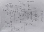
Ckt2.jpg

This is the bridge circuit...

Ckt1.png

Oscilloscope screenshots of controller outputs to the gate driving transformer primaries...
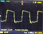
Scope1.png

Scope2.png
 

The observed behaviour can easily happen if one transistor pair is soft and the other hard switching at the actual bridge phase shift. How do you guarantee ZVS operation over the intended operation range?
 
the magnetising current decays in the shorted Tx wdg, and there is not enough energy left to soft switch the leg you refer to, solutions are listed in literature, including an aux choke in series with the Tx pri and extra clamping diodes to reduce voltage overshoots, kind regards,
 
Thank you very much to both of you.

FvM, I should admit I didn't know how ZVS is guaranteed. This is a circuit not designed by me, but I got it from somewhere else. I am still learning about this topology.

Easy peasy, if this is the issue, shouldn't it affect both the legs? How come it affects only one leg?
 

Hello,

I have an arc lamp power supply board which has a zero voltage switching full bridge converter circuit, utilizing UC3875 controller and IRF840 power MOSFETs. Input voltage is 230V which goes to a PFC circuit which provides 400V for the bridge. OUTA and OUTB terminals of the UC3875 drives one transformer (MOSFETs gate drive for one leg of the bridge). OUTC and OUTD terminals drive another transformer driving the two MOSFETs of the other leg of the bridge. Output voltage is 18V.

It works well for 8A load current. But when I increase it to 12A, only two MOSFETs (One upper and the other lower, of the same leg) are overheating and getting fried in a few minutes of operation. The two MOSFETs of the other legs looks okay.

One observation is that the MOSFETs which are overheating are always those driven by the transformer which is connected to OUTC and OUTD terminals of UC3875. MOSFETs driven by the transformer connected to OUTA and OUTB are fine. When I interchanged the transformer primary connections to UC3875, this held true and the overheating shifted to the other leg's MOSFETs.

I tried increasing the dead time, but it made no difference. Could anyone please suggest how to approach this issue?

This is the controller circuit...

View attachment 159268

This is the bridge circuit...

View attachment 159269

Oscilloscope screenshots of controller outputs to the gate driving transformer primaries...
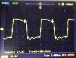
View attachment 159270

View attachment 159271

This is a common phenomenon in a PSFB ZVS converter. I expect the heating issue in the lagging leg due inadequate inductive energy to discharge the mosfet o/p capacitance. They are getting hard-switched

I am not seeing any leakage inductance to aid in ZVS process also.

1)When i look up the Mosfet datasheet, It shows it has VDS_Breakdown =500V..For 400V applications, it is slightly marginal. Also the reverse recovery charge & time for body diode is a little higher which may create problems in body diode recovery. Please use a 600V Mosfet with a faster body diode .

2)I am seeing a only Capacitive snubber across a mosfet. During ontime, it dumps all stored energy into the mosfet. Please use a RCD snubber.

3)Estimate the dead time. It should be Tdead= (1/4) * pi*SQRT(Ls * Cs)
 
Thank you biswaIITH.

I was thinking the MOSFETs of both the legs are subjected to the same stress, and if the transformer inductance is insufficient to attain ZVS, both the legs should become overheated. But when you mentioned 'lagging leg', I did a Google search and found one pair is called leading leg and the other lagging leg. So there must be some differences in the power dissipation between them. Could you please suggest an article or something which explains this difference?

I made an inductor, winding copper wire around a toroid and connected it in series with the transformer primary. But the core overheated and broke. There was no reduction in the MOSFET heating either.

I have ordered IPA60R170CFD and IPP60R070CFD MOSFETs (600V models with fast body diode). Do you think these MOSFETs can make a difference?

Does an ZVS require snubbers?

I have increased dead time to very high levels but it made no difference in the heating.

1)Please search in google. You will get very good app notes from Texas Instruments, Vishay, ST etc. See basically ,during lagging leg transition, inductive energy is not sufficient to discharge the Mosfet o/p cap. Kindly, go through any TI app note to understand the concepts of ZVS in PSFB .

2)Before designing the inductor, kindly follow some basic guidelines(You can refer any design note/text book). Calculate the inductor value. Use Ferrite cores & Litz wire(IF high switching frequency) for its design. Check its core area product, Peak current flowing through it, Current density etc. I assume you know how to calculate resonant tank current in PSFB.

3)Yes CFD series Mosfets are really good for this applications

4)ZVS in PSFB removes only turn-on losses but if you keep a snubber across a Mosfet, it will reduce the turn-off losses as well.

5)Ensure a) (0.5*Ls* Ipeak^2) > (0.5* Coss(total) *V^2)
b) T_Dead= (1/4)*(2*Pi* SQRT(Ls *Ctotal) for ZVS

My suggestion is do a thorough calculation before proceeding to the design
 
Last edited:
one pair is called leading leg and the other lagging leg. So there must be some differences in the power dissipation between them. Could you please suggest an article or something which explains this difference?

Try researching and reading Unitrode app notes - there is a lot of information out there on FBPS - full bridge phase shift

In simple terms, after power pulse there is current in the Tx, this leakage inductance energy is sometimes enough to give ZVS when the next fet turns off, then there is a period when the Tx pri is shorted and the current / energy in the leakage falls, thus there may not be enough energy for ZVS at the next transition ...
 
Status
Not open for further replies.

Part and Inventory Search

Welcome to EDABoard.com

Sponsor

Back
Top