Continue to Site

Welcome to EDAboard.com

Welcome to our site! EDAboard.com is an international Electronics Discussion Forum focused on EDA software, circuits, schematics, books, theory, papers, asic, pld, 8051, DSP, Network, RF, Analog Design, PCB, Service Manuals... and a whole lot more! To participate you need to register. Registration is free. Click here to register now.

[SOLVED] Mosfet ringing at switch ON step

Status
Not open for further replies.

Monolith

Junior Member level 1
Joined
Sep 21, 2009
Messages
16
Helped
0
Reputation
0
Reaction score
0
Trophy points
1,281
Location
Switzerland
Activity points
1,415
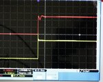
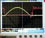
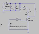
When I switch the IRFP640 N Mosfet ON, I get some ringing. My guess is that this is due to the Miller effect.

How can I avoid it?
 

Switch it on slower by rc filtering the gate ....but maybe the ringing does not matter, do you have scope shot? schem?
 
Hi,

Maybe a impedance problem.

The loop: FET source - driver GND - driver Vcc capacitor - driver output - to FET gate. And bootstrap circuit.
Needs to be very short, wide traces, low inductive.

A low inductive resistor in the gate line could improve stability.

Klaus
 
also beware of scope noise...esp when you have long dangling ground hook.
 
Scope picture shows Mosfet driver output, yellow, Mosfet gate red trace. ON voltage about 13V.

- - - Updated - - -

Yellow trace is Flyback, red trace is gate voltage.

Trying to switch at 0 Volt, ZVS
 

Attachments

  • Gate ringing.jpg
    Gate ringing.jpg
    108 KB · Views: 134
  • Flyback and gate.jpg
    Flyback and gate.jpg
    145.1 KB · Views: 128

Firstly. A certain impact of miller effect is normal operation. What's your specific problem with it?

Secondly. We need to see the actual gate driver circuit to understand how far "driver ouput" can be different from "Mosfet gate" voltage. Ringing suggests existence of wiring inductance, which can be generally considered "avoidable". But may be not avoidable for your design.

- - - Updated - - -

The new waveform needs additional explanation respectively circuit information.

If this is actually drain-to-gate crosstalk (could be, because the capacitance is very nonlinear and considerably increasing near Vds = 0), there's apparently a problem of too high gate driver impedance.
 
This is the simplified LTSpice simulation circuit. The actual circuit uses a Mosfet driver MIC4452

- - - Updated - - -

Firstly. A certain impact of miller effect is normal operation. What's your specific problem with it?

Secondly. We need to see the actual gate driver circuit to understand how far "driver ouput" can be different from "Mosfet gate" voltage. Ringing suggests existence of wiring inductance, which can be generally considered "avoidable". But may be not avoidable for your design.

- - - Updated - - -

The new waveform needs additional explanation respectively circuit information.

If this is actually drain-to-gate crosstalk (could be, because the capacitance is very nonlinear and considerably increasing near Vds = 0), there's apparently a problem of too high gate driver impedance.

Thanks for the replies.
Yes, it is a crosstalk problem. The gate driver is supposed to give 12A peak current at 18V, (but running at 13V now) however, adding 10 Ohm in series seems to give less ringing.
 

Attachments

  • Mosfet circuit.jpg
    Mosfet circuit.jpg
    43.5 KB · Views: 162

Then it's primarly a wiring inductance problem, I think.

Thanks for the help.
This problem occurs on the prototype perforated circuit board. Distance of the Mosfet driver to the gate is about 40mm. Resistor length of about 20mm is included in that. Now drawing a PCB, SMD, with minimum distance between driver and gate. Trying to avoid the problem.
 

Hi,

Resistor length of about 20mm is included in that.
What resistor? Could it be a high impedance wire wound resistor?

Klaus
 

Hi,


What resistor? Could it be a high impedance wire wound resistor?

Klaus

I had a wirewound resistor of 1.8 Ohm and got oscillations. Changed to what I think is a carbon 3W, 10 Ohm resistor which gives what you see on the pictures. Tried several different kinds of Mosfets. Each kind behaves a little different.
 

Hi,

don´t use wirewound.

Klaus
 

Im unable to locate a resonance frequency of about 2 MHz in the gate circuit, would require several µH wiring inductance which isn't feasible.

I think, we see something completely different, a resonance of the 40 nF capacitor with a 150 nH capacitor ESL + ground loop inductance, series resonant circuit closed through the MOSFET. It's coupling to the gate circuit, or at least your gate voltage probe.

We should look at the topic again when you have finished your final design with regular PCB wiring.
 

Impedance control gives best control of ringing due to transient CISS during transition.

THe ratio of source to switch to load impedance has a penalty of rising CISS with lower RdsOn.
I prefer to choose a ratio of 50:1 max from driver to switch impedance. Then asymetry is another choice due to shoot thru, so lower impedance turn off and higher turn on is preferred to assist in dead band of complementary drivers or half bridge.

Then use very short leads or none with coaxial pin and ring of 10:1 probe.

Also make sure C4 is very low ESR/low ESL path. ( <<10mΩ) such as film.
 
Thanks for all the good advice.

Smooth, noiseless switching is very important for my application.

Some of the new SiC Mosfets apparently have much less Miller effect. Is there anybody with experience in using these?

What about using 2 Mosfets in Cascode?
 

Status
Not open for further replies.

Similar threads

Part and Inventory Search

Welcome to EDABoard.com

Sponsor

Back
Top