Continue to Site

Welcome to EDAboard.com

Welcome to our site! EDAboard.com is an international Electronics Discussion Forum focused on EDA software, circuits, schematics, books, theory, papers, asic, pld, 8051, DSP, Network, RF, Analog Design, PCB, Service Manuals... and a whole lot more! To participate you need to register. Registration is free. Click here to register now.

MOSFET output stage for digital amplifier

Status
Not open for further replies.

Mnt

Member level 5
Joined
Mar 20, 2016
Messages
91
Helped
2
Reputation
4
Reaction score
2
Trophy points
8
Activity points
721
I want to build a class D amplifier which is supplied by 100Vdc single supply and another 12V supply.

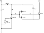
I've tested this output stage in Multisim but there is cross conduction.
Mine input signal is 0V-12V 75khz.

Help me to design an output stage without cross conduction, MOSFET driver IC and without dual supply.

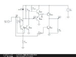
HELP.PNGNICE.PNG

- - - Updated - - -

This is variant 2 of this.
This time another problem -> output probe shows 257 Mhz and simulation stopped due to convergence issue. :x
HELP_VARIANT_@.PNG

- - - Updated - - -

I found a error in my 2nd schematic.
This is the corrected one but it has cross conduction. The cross conduction its less than the first schematic.
HELP_WAY_BETTER.PNG

- - - Updated - - -

I succedded to drop the cross conduction more but its problem again.
Look at the oscilloscope. One channel is input, other is high side gate.
Looks bad.

**broken link removed**
 

I am very close and cant get it. :(

HARD.PNG
 

I'm running a simulation. Single ended supply. Operation is class A. (Your output stage is not connected. Therefore I assume your schematic is supposed to connect C1 to the node between the mosfets?)

Notice that C1 is the sole agent pulling current through the output stage during one-half of the cycle. (Furthermore it blocks the DC component.)

However it does not deliver adequate power, unless the mosfets conduct in both directions, up and down. You really need a split supply, so that the positive supply is an active agent propelling current during one-half of the cycle, and the negative supply is the active agent during the other half of the cycle.

Furthermore C1 creates resonant behavior, along with L1 & C2. Add the switching action of upper & lower mosfets. The result can be high-voltage spikes which are liable to destroy components.
 

Output filtering is not connected because im testing only the output stage, not the filtering.

However it does not deliver adequate power, unless the mosfets conduct in both directions, up and down. You really need a split supply, so that the positive supply is an active agent propelling current during one-half of the cycle, and the negative supply is the active agent during the other half of the cycle.

Furthermore C1 creates resonant behavior, along with L1 & C2. Add the switching action of upper & lower mosfets. The result can be high-voltage spikes which are liable to destroy components.

You say its not possible with single supply, but its possible.
I tested with IR2110 and 2x IRF640 and IT WORKS.

But I want to not use the IC.
 

You're going to have a lot of trouble getting good results by using so many BJT circuits. Each one has different rise and fall times, which makes it very hard to get the timing of the final outputs to align well. I certainly hope this is just a one-off project, because this certainly won't work for a manufactured problem.

There's good reason people use bootstrapping ICs like the IR2110. They're generally the cheapest and simplest option.
 

I thinked the BJTs are fast :D
 

BJT are fast if not driven into saturation. In addition MOSFET gate driver must provide low impedance push-pull operation, particularly fast gate discharge. That's impossible with your single transistor high side driver circuit. Just helpless.
 
  • Like
Reactions: Mnt

    Mnt

    Points: 2
    Helpful Answer Positive Rating
Is 2n7000 or bs170 more fast than a BJT or BJT is faster ?

I found these on the net.

DriverCircuit.PNGBootstrapped Mosfet.PNG
haha.png
 

Hi,

Have you had a look at "Design and Application Guide for High Speed Mosfet Gate Drives," or "Low Saturation Transistor for Gate Drive Application," (OnSemi AND9285/D), or "Chapter 5 Gate and Base Drive Circuits and Protection."

I don't know much at all, I'm just looking into this area now as I'm curious about SEPICs, but maybe things like totem-pole gate drivers and (possibly, but not necessarily) "Baker collector clamping circuit" could be of assistance?

- - - Updated - - -

The datasheets will say the rise, delay/storage and fall times.
 
  • Like
Reactions: Mnt

    Mnt

    Points: 2
    Helpful Answer Positive Rating
Thanks for these references, will look them.

What about redesigning this output stage to single supply one ?
200W-class-D-amplifier.jpg
 

Status
Not open for further replies.

Similar threads

Part and Inventory Search

Welcome to EDABoard.com

Sponsor

Back
Top