Continue to Site

Welcome to EDAboard.com

Welcome to our site! EDAboard.com is an international Electronics Discussion Forum focused on EDA software, circuits, schematics, books, theory, papers, asic, pld, 8051, DSP, Network, RF, Analog Design, PCB, Service Manuals... and a whole lot more! To participate you need to register. Registration is free. Click here to register now.

MOSFET current control

Status
Not open for further replies.

parth22

Member level 4
Joined
Mar 15, 2022
Messages
78
Helped
2
Reputation
4
Reaction score
1
Trophy points
8
Activity points
518
HI all,
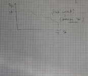
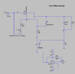
I have this below mentioned circuit. Here I would like to charge the capacitor but in steps. And these steps will be based on the Vds of MOSFET.(it can be seen in the second image).
I have a shunt resistor (R1) either 1mohm or 2 mohm. So to turn on the NPN, I need atleast 700mV so using a amplifier circuit. (one can modify it or change it).
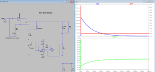
Maximum current flow is 1 to 6A.
can anyone tell why I am getting so high peak current or how can I adjust this circuitry.
 

Attachments

  • image_4.png
    image_4.png
    58.8 KB · Views: 124
  • 1653551562215.jpg
    1653551562215.jpg
    232.1 KB · Views: 117

The step response of an RC circuit to a V step is inherently impulse like for
small R. Aggravated by AD549 slew rate and bandwidth (delay in the control
loop).

Basically a differentiator response.

1653645101573.png


If step change is a step change in current then response is a ramp.


Regards, Dana.
 

Hi,

The whole circuit makes no sense to me.

Please describe each part .. at least briefly.
I see many problems. like
* output of OPAMP short circuited to 3V3
* no power supply bypass capacitors
* no local feedback capacitors to ensure stability
* no base resistor
* no emittter resistor
* too high ohmic RG
* OPAMP supply voltage range
* ...

Klaus
 

The AD549 has an output that has short circuit current limit of 35 mA. So not best practice to
not use a base current limiting R, however circuit probably still work. But no R in this
case, transistor deep in saturation, aggravating the control loop delay problem.

The MOSFET can conduct considerable current at low Vgs

1653647430341.png


But the AD549 has crappy output swing at a Vs of 3.3V. Or raise its supply V. Would be better to use a rail-rail output OpAmp.

1653647605446.png


Regards, Dana.
 

The AD549 has an output that has short circuit current limit of 35 mA. So not best practice to
not use a base current limiting R, however circuit probably still work. But no R in this
case, transistor deep in saturation, aggravating the control loop delay problem.

The MOSFET can conduct considerable current at low Vgs

View attachment 176399

But the AD549 has crappy output swing at a Vs of 3.3V. Or raise its supply V. Would be better to use a rail-rail output OpAmp.

View attachment 176400


Regards, Dana.
SO can you give a modified scatch?
--- Updated ---

Hi,

The whole circuit makes no sense to me.

Please describe each part .. at least briefly.
I see many problems. like
* output of OPAMP short circuited to 3V3
* no power supply bypass capacitors
* no local feedback capacitors to ensure stability
* no base resistor
* no emittter resistor
* too high ohmic RG
* OPAMP supply voltage range
* ...

Klaus
Okah so for a while see the circuit like this. (attached).
Now you can see I need 700mV at the base of NPN but I am using a current sense resistor R1 that is 2mohm and let's suppose maximum current is 1A then we have only 2mV but this can not turn on the NPN and will not shut off the MOSFET.
Target is: to charge the capacitor with 1A and (that 1A is sense by shunt resistor) and shut off the MOSFET.

Rest you can edit circuit as you want. I mean put component which is required.
 

Attachments

  • image_5.png
    image_5.png
    15.6 KB · Views: 95
Last edited:

SO can you give a modified scatch?

Whats a scatch ?

Youi could use the MOSFET as a switch, and in its source to cap create a
cons current source, say using a LM317.

1653650583155.png


Add this and add a diode to its output so that when MOSFET is off the LM317
does not discharge the Cap.


So you have MOSFET Source >> LM317 Current Reg >> Diode >> Cap >> ground

for the circuit. <MOSFET just acting as a switch.

How high a V does the Cap need to get charged to ?

Here is a simple sim. Not at 1A yiour 1`.5 uF cap charges quickly, is that what yiou want ?
Also not the LM317 takes a few mS to start up, but once it does its acting as a constant
current.

1653652485987.png


Here is same sim but with 1.5F cap, is this more what yiou are looking for ?

1653652607745.png


Regards, Dana.
 
Last edited:

Whats a scatch ?


Regards, Dana.
that schematic..
--- Updated ---

Whats a scatch ?

Youi could use the MOSFET as a swiutch, and in its source to cap create a
cons current source, say using a LM317.

View attachment 176408

Add this and add a diode to its output so that when MOSFET is off the LM317
does not discharge the Cap.


So you have MOSFET Source >> LM317 Current Reg >> Diode >> Cap >> ground

for the circuit. <MOSFET just acting as a switch.

How high a V does the Cap need to get charged to ?


Regards, Dana.
Cap will charge upto 42V.
Whats a scatch ?

Youi could use the MOSFET as a switch, and in its source to cap create a
cons current source, say using a LM317.

View attachment 176408

Add this and add a diode to its output so that when MOSFET is off the LM317
does not discharge the Cap.


So you have MOSFET Source >> LM317 Current Reg >> Diode >> Cap >> ground

for the circuit. <MOSFET just acting as a switch.

How high a V does the Cap need to get charged to ?

Here is a simple sim. Not at 1A yiour 1`.5 uF cap charges quickly, is that what yiou want ?
Also not the LM317 takes a few mS to start up, but once it does its acting as a constant
current.

View attachment 176409

Here is same sim but with 1.5F cap, is this more what yiou are looking for ?

View attachment 176410


Regards, Dana.
so first I don't have choice to use LM317 voltage regulator. And I am charging the cap to the supply voltage. while in your simulation cap will be charged upto 3V, while supply is 12v. That's not my intention.
I only want to use a single NMOS as an current limiter and that current will be sensed by shunt resistor. and NPN circuit is used to fast switch off the NMOS, once the cap is charged.
Although the expected result will be the same as you got.
so for circuit : NMOS (supply to the drain and output source) >> cap (with a Resistor load)>>shunt resistor.
gate of NMOS to shunt resistor a NPN circuit for switch off. any opamp for amplification the shunt resistor voltage. or some switches (NPN) that will work based on the Vds of NMOS.
like if Vds<40V, I_shunt_res. = 120mA
if Vds < 30V , I_shunt_res = 500mA
if Vds< 20V , I_shunt_res. = 1A
if vds< 10V, I_shunt_res = 2A.
(so these are the steps, i can reduce or increase)
 
Last edited:

I do not like the sim results. The LM317 requires too much V across it to stay in
current regulation. I tried it with a LDO regulator, that worked better but also seemed
to be in oscillation.

When you pump up cap :

1. Whats max V you will pump it to ?
2. Are you pumping at a 1 Khz rate ?
3. Is cap just 1.5 uf ?

Regards, Dana.

OK, I see your comments above prior to this post.
 

I do not like the sim results. The LM317 requires too much V across it to stay in
current regulation. I tried it with a LDO regulator, that worked better but also seemed
to be in oscillation.

When you pump up cap :

1. Whats max V you will pump it to ?
2. Are you pumping at a 1 Khz rate ?
3. Is cap just 1.5 uf ?

Regards, Dana.
Don't use any voltage regulator or LDO something.
1. 42V
2. i don't know about frequency
3. 1.5mF
**** (please check the pictures of 1st post again)
 

Still confused about what you think the circuit should be (seems rather convoluted) and what you actually want the circuit to do (not always the same).

Below is the LTspice simulation of a simple constant-current circuit that will charge the capacitor to the 42V supply voltage:
The charge current is approximately 0.7V / R1.
Transistor M2 turns the circuit on and off.

1653675353728.png
 
Last edited:

Still confused about what you think the circuit should be (seems rather convoluted) and what you actually want the circuit to do (not always the same).

Below is the LTspice simulation of a simple constant-current circuit that will charge the capacitor to the 42V supply voltage:
The charge current is approximately 0.7V / R1.
Transistor M2 turns the circuit on and off.

View attachment 176417
@crutschow
Thanks for this but same phenomena I would like to achieve with NMOS(M1). There you can use an opamp for gate control and npn for fast discharge.
So any suggestion?
 

In a short, the post #1 simulation circuit has several flaws that make it behave as it does. A few modifications make the simulation basically work, the control loop is however at the stability margin. At should be also noted that AD549 isn't specified to work with +/- 3.3V supply. You'd select a suitable OP instead.

If you want others to check and correct your LTspice simulation circuit, please post a .zip archive of the simulation files (.asc, .plt, nonstandard component libraries if any).

1653898225847.png
 
In a short, the post #1 simulation circuit has several flaws that make it behave as it does. A few modifications make the simulation basically work, the control loop is however at the stability margin. At should be also noted that AD549 isn't specified to work with +/- 3.3V supply. You'd select a suitable OP instead.

If you want others to check and correct your LTspice simulation circuit, please post a .zip archive of the simulation files (.asc, .plt, nonstandard component libraries if any).

View attachment 176455
@FvM
you have done right simulation that also I have done.
But results are not expected. Vout should be reached till 42V. you can choose another opamp that work with 3,3V. expected result is something like (posted in post 10).
control loop is made to increase the gain.
 

Hi,

in post#3 I showed 7 issues.
Until now I don´t see that you removed a single one.

All schematics, modifications, simulations came from forum members. I don´t see any effort from your side.

If you want others do your job, then consider to pay someone.

Klaus
 

1. control loop must have sufficient phase margin which is obviously not the case => design appropriate loop compensation
2. circuit startup is another problem which causes the huge current peak in original design
 
So any suggestion?
Since I still don't understand (and you have not clearly stated) the exact purpose of your funky circuit (why charging in steps?), and why you insist on using it (other than it's the one you designed), I'll leave dealing with that to others.
 
Last edited:

Since I still don't understand (and you have not clearly stated) the exact purpose of your funky circuit (why charging in steps?), and why you insist on using it (other than it's the one you designed), I'll leave dealing with that to others.
To keep within the SOA region of NMOS. As per the SOA, at high voltage we need less current so what i am looking is continuous current steps.
the idea behind is like initially some current that will charge up the cap, then some more current will come then it will charge the cap and then final current step will fully charge the cap. it's something ladder of current. and FYI, current profile will come from SOA of NMOS.
 

@crutschow
Thanks for this but same phenomena I would like to achieve with NMOS(M1). There you can use an opamp for gate control and npn for fast discharge.
So any suggestion?
AFAIK N-channel MOSFETs don't have any advantage over P-channel devices regarding SOA limits, so why do you want to use N-channel?
 

To keep within the SOA region of NMOS
An NMOS will not charge the cap to the full 42V unless you have a higher bias voltage for the MOSFET, so a P-MOSFET would be better.

It would be simpler just to select a MOSFET with a sufficient SOA so you wouldn't have to step the current.
 

Hi,

Pulsed current just reduces the average current.
If you reduce the DC current you don't need pulses.

I see no benefit for the pulsed operation, it just is more complicated and increases noise.
The same is with the N-MOS ... it just overcomplicates the circuit.

Klaus
 
Status
Not open for further replies.

Similar threads

Part and Inventory Search

Welcome to EDABoard.com

Sponsor

Back
Top