Continue to Site

Welcome to EDAboard.com

Welcome to our site! EDAboard.com is an international Electronics Discussion Forum focused on EDA software, circuits, schematics, books, theory, papers, asic, pld, 8051, DSP, Network, RF, Analog Design, PCB, Service Manuals... and a whole lot more! To participate you need to register. Registration is free. Click here to register now.

MOS switch-missing important concept, needs help

Status
Not open for further replies.

yawijaya

Member level 2
Joined
Aug 18, 2009
Messages
42
Helped
0
Reputation
0
Reaction score
0
Trophy points
1,286
Location
New Freedom, PA-USA
Activity points
1,625
mos switch

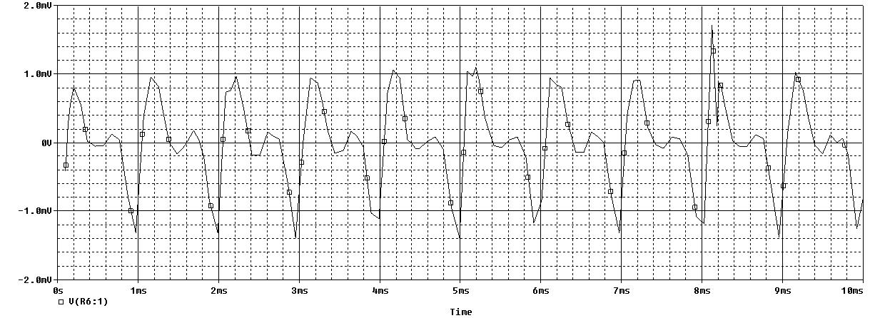
I learned this a while back when i was in college, and now i need to re -learn this again...anyway, please take a look at the picture
85_1251125732.jpg

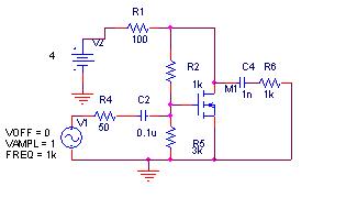
For what i know this circuit should give me an output either the top or bottom half of the input sinusoidal wave. The datasheet of the transistor says that vgs is 2-4V. but my output is just not what i expected.


I think i'm missing one important concept but can't recall it..ANy suggestion?Thanks for the help!
 

nmos vs pmos switch

The value of the 1nF capacitor C4 is much too small to pass 50Hz to the 1k load resistor R6 so it passes only the very high frequency distortion. Use 100uF.

The Mosfet has a gate threshold voltage of 2V to 4V where it barely turns on with 250uA. The resistors R2 and R5 bias the gate at 3V. Then the Mosfet might conduct or it might not conduct.
 

    yawijaya

    Points: 2
    Helpful Answer Positive Rating
design a nmos switch

Thanks for the reply, but what i'm concerned is that i want it to act as switch to take the top half of the input signal out.How am i supposed to do it?Thanks
 

mos switch matrix

The gate threshold voltage for the Mosfet is a wide range of voltages. You must adjust the gate voltage with a pot to do what you want. Then the Mosfet turns on hard and saturates when the input signal is positive and it amplifies and passes the signal when the input is negative.
 

    yawijaya

    Points: 2
    Helpful Answer Positive Rating
MOS switch

a few suggestions:

1) you should have higher supply rail: a mosfet needs a minimum of 4-5v Vds to operation as a linear amplifier. I would increase V2 to more like 9 - 12v, or more, ,depending on your application.

2) you should also put a small resistor (like 11 - 47ohm) between the mosfet's source and ground to help define the gain.

3) you need to reside your capacitors for the kind of signal you want to amplify.

4) you should adjust the bias resistors (R2/R5) so that the output obtains the maximum symmetrical swing. That means that for your topology, the drain should sit at Vds(min) + (V2-Vds(min))/2. assuming V2=9v, Vds(min)=5v, that means the drain of the mosfet should be at 7v, and the amplifier can swing +/- 2v max - likely less.

you can then calculate its working points at idle.
 

    yawijaya

    Points: 2
    Helpful Answer Positive Rating
Re: MOS switch

Hi, thanks a lot, the last one really helps!anyway, what should you do if the datasheet doesn't tell the minimum VDS, it says that typical is 10 or 12.5 V, but that's high though...
 

MOS switch

The VDS can be anything. The Vgate is the one that controls how much the Mosfet turns on and every Mosfet is different.
 

Re: MOS switch

ok, so if i get it right, i need to find out how many Id i want and then check on the current-volt curve to see which vds i need and then i can calculate for the Vgate..is that correct?
 

Re: MOS switch

yawijaya said:
Hi, thanks a lot, the last one really helps!anyway, what should you do if the datasheet doesn't tell the minimum VDS, it says that typical is 10 or 12.5 V, but that's high though...

the minimum Vds will depends on how much distortion you will tolerate. most mosfets are designed for switching applications, and they want their devices to be in saturation.

for linear application (where you are now), that's not what you want to do. instead, you want to have ample headroom to control the output voltage so it doesn't clip. the 4-5v number I provided you is quite good even for high power applications and is conservative for small signal applications (like yours).

you can design for higher Vds(min) but you may not gain enough to justify the added cost (inefficiencyy, heat dissipation, high voltage components, etc.)

i need to find out how many Id i want and then check on the current-volt curve to see which vds i need and then i can calculate for the Vgate..is that correct?

generally no. for a single-ended small signal amplifier like yours, you want to figure out what the worst load it will be driving. it looks like you are designing an audio amplifier, and your load is likely a preamp. They tend to have a minimum input impedance of 470ohm and usually much higher than that (4.7k or higher).

so if you design to drive a 470ohm load (worst case scenario), you want your output impedance (R1) to be no greater than the load. I typically design so that R1 is 50% - 10% of the load. that means R1 is 220ohm or lower.

once you have that, you will determine the gain of your amp. It is (R1//Rload) / Rs where Rs is the resistor between the source of the mosfet and the ground. say that you want to achieve a gain of 2x, that means (220//470)/2x=68ohm (rough math). that math assumed a mosfet with infinite gain so in real world we will likely have a lower gain thus may require a lower Rs to compensate.

the input impedance is roughly R2//R5. if you are running at a 9v rail and your Vd sits at about 7v. since the mosfet needs Vgs=3-4v to open so the R2/R5 divider will attenuate Vd by a factor of 2x so R2=R5. That means your input impedance is 1/2*R2.

I usually design my amp to have input impedance of no higher than 47k and no lower than 4.7k and typically around 10k so R2=R5=22k.

R4 is there for stability and I will keep it at 1k. you can choose the capacitors to suit your needs - mostly frequency response related. I usually use 0.22u - 0.47u for C2 and 4.7u - 47u for C4.

so here is the final design.

as you can see, it provides reasonably good performance. the gain is slightly less than 2x, due to an imperfect mosfet as well as attenuation caused by R4 (in your schematic).

after this, you will need to figure out its frequency response (ac analysis) to make sure that a) it doesn't oscillate and b) it fits your needs.
 

MOS switch

you will find that the drain of the mosfet doesn't sit at 7v - in my example, it sits at 8v - as the working point is dependent on the mosfet's Id vs. Vgs relationship.

so for amplification of large signal, the clipping may not be as symmetrical as we had expected.

Obviously, that's not a big deal for small signal amplification. But if you really want to have symmetrical clipping, you can adjust R3/R4 (in my schematic) so that Vd sits at your desired level.

as R3//R4 determines your input impedance, you don't want its adjustment to lower your input impedance. As such, you should aim to INCREASE R3 or R4 as appropriate.

you should also try to select a mosfet that fits your needs in terms of Id and Vds(breakdown). But also its input capacitance. try to lower the input capacitance (Ciss in most datasheet) to less than 220pf.

small signal mosfets work really well here, particularly the superline ones from Zetex. IRF510 is a medium power mosfet but surprisingly has very low Ciss, and it is quite inexpensive and readily available so I use it a low for either preamp or headphone amp.

one remarkable thing about this particular topology is the bias stability with regardes to supply rail.
 

Status
Not open for further replies.

Similar threads

Part and Inventory Search

Welcome to EDABoard.com

Sponsor

Back
Top