Continue to Site

Welcome to EDAboard.com

Welcome to our site! EDAboard.com is an international Electronics Discussion Forum focused on EDA software, circuits, schematics, books, theory, papers, asic, pld, 8051, DSP, Network, RF, Analog Design, PCB, Service Manuals... and a whole lot more! To participate you need to register. Registration is free. Click here to register now.

MOS resistor linearization technique

Status
Not open for further replies.

Junus2012

Advanced Member level 5
Joined
Jan 9, 2012
Messages
1,552
Helped
47
Reputation
98
Reaction score
53
Trophy points
1,328
Location
Italy
Activity points
15,235
Hello,

is it possible to linearize the MOS resistor by using a poly resistor in parallel to it ?
please refer to the below picture, the author is running the filter by varying the gate of the transistor while he kept a resistor in parallel,
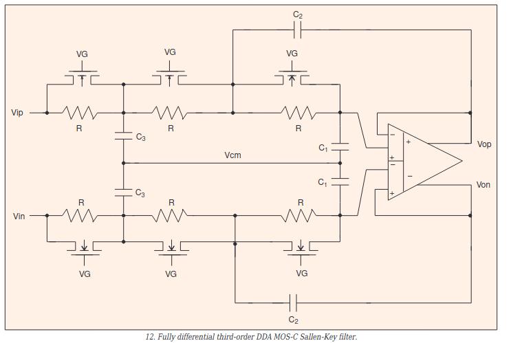
rmos.jpg


In my opinion, if i want to cancel the non linearity if the NMOS then I must connect a device with opposite charasteritcis, while the poly resistor is linear, I am not sure how it is working


thanks
 

Switched poly resistor segments FTW. Granular enough
to control by code, not by MOS parallel resistance
"analog style", as those would still be nonlinear (even
if second-order scale)

To linearize MOS you'd need to keep each segment in
its linear region (Vds << Vgs) and also deal with body effect
if that varies along the stack (love SOI, problem for JI).
 

    Junus2012

    Points: 2
    Helpful Answer Positive Rating
Such construction is less linear for sure. I can imagine that mosfets are used here for trimming cut off frequency in limited range.

I have seen integrators uses M-2M ladder as current divider at the opamp input. However, such technique provides linear current division not linear resistance.
 

    Junus2012

    Points: 2
    Helpful Answer Positive Rating
For sure such parallel combination of MOS and poly resistors will still be non-linear, but how much nonlinear compared to a MOS resistor only. It looks to me that if the poly resistor has smaller resistance than the MOS, it will tend to reduce the non-linearity. I think like that because if we take it to the extreme, where the poly resistor is much smaller than the MOS resistor, then the parallel combination effective resistance will be defined by the poly resistor and hence will have the linearity of the poly resistor. At the other extreme where the poly R is much bigger than the MOS R, obviously the MOS R will dominate with all its non-linearity. So, somewhat smaller poly R in parallel may have the effect of reducing the overall non-linearity, but not cancelling it.
 

    Junus2012

    Points: 2
    Helpful Answer Positive Rating
Thank you dear friends for your answer,

your answer was useful, the non-linearity can be reduced but not canceled, also depends on which of the resistors are dominating

I have tested that by simulation and run the THD to compare

I have one issue, I usually rated your answer 'helped me' but when I open the post again it looks like I didn't rate it. I am surprised to see that with all of my history post. I don't want to look like non grateful man who only take an answer and leave no rate, so please tell me if you are not receiving my rating

Thanks
 

Don't worry. I guess we are not here for the rating. But yes, your helpful rating id there, I can see it.

What were the results of your THD simulations?
 

    Junus2012

    Points: 2
    Helpful Answer Positive Rating
Don't worry. I guess we are not here for the rating. But yes, your helpful rating id there, I can see it.

What were the results of your THD simulations?
it was without R -44 dB and with R is -51 dB
--- Updated ---

it was without R -44 dB and with R is -51 dB
I am fedup of using CMOS filters, I think Gm-C filter is better
 

OK, 7dB difference. Not bad, but higher power consumption.
I am not sure if Gm-C would be better. It depends on the frequency of operation and how much degeneration you can have. Gm-C can reach higher frequencies, with maybe -40dB or -50dB of linearity. Opam-RC are supposed to work with better than that distortion.
 

    Junus2012

    Points: 2
    Helpful Answer Positive Rating
it was without R -44 dB and with R is -51 dB
These numbers doesn't look good. The most probably because of use mosfets as resistors.
If we consider opamp with 60dB OL gain, 3V output swing (so 3mV directly at input), differential pair in moderate inversion generate -95dB of HD3, so if we add 20dB of other sources in opamp, it is still 20dB above.
 

    Junus2012

    Points: 2
    Helpful Answer Positive Rating
I am seriously thinking iof using the gm-C filter
I will tell you my experience,

I went for MOSFET -C filters because the tunning range is very wide from low 50 Hz to 5 MHz, and I was not sure if you can stress the gm to cover this band.
So for me linearity was not expected to be good when I used the MOSFET-C, it is comparable to the Gm-C ... but here I could tune it for the required bandwidth.

If you think that still gm-C filter can afford such tunning range, then I am keen to start working on it


Thank you
 

You need to tune current by 5 orders of magnitude. If you make such bias circuit working than Gm-C cut off frequency tuning be also working.
 

    Junus2012

    Points: 2
    Helpful Answer Positive Rating
By the way friends, my filter circuits work fine until I layout the feedback capacitors, then performance start to degrade, and some times too much. my circuit is similar to the one in post one.

I am using poly1-2 CAPs.
I extracted the design with only R and no problem.

My minimum C unit is 0.9 pF, which I was thinking that is far away to be affected by parasatics,

I am using symetrical output routing

Is using metal cap can produce less parasitic?

Thanks
 

What does it mean? Your cut off freq is lower or something else?
The cutoff frequency and the transfer function as well,
so the simulation before cap layout was showing me roll off = -76/decade, but after layouting the caps it becames -68 dB/ decade.. which means my filter is no more butterworth.
 

Ok, so nothing special.
Annotate parasitic, add them to schematic and compare results.
If the same, then trim your poly caps to get proper results. Redraw, reextract, resimulate.
 

    Junus2012

    Points: 2
    Helpful Answer Positive Rating
Ok, so nothing special.
Annotate parasitic, add them to schematic and compare results.
If the same, then trim your poly caps to get proper results. Redraw, reextract, resimulate.
Thank you Dominik,

That is what I am right now doing, I am tunning Q by trimming the Caps to correct the filter response

with butter worth I now reached to these value but not finished layout yet

Q1= 0.665 , Q2 = 1.581
while original ideal values are

Q1= 0.512, Q2 = 1.3065,

For this values I am using

1st biquad C2 = 1.0375pF*8
C1= 966 fF*5


2st biquad C2 = 1p*20
C1= 1pF*2

The matching array is

[C2.1........C2.10, C1.1]2nd biquad [C2.1........C2.4, C1.1-C1.5, C2.5........C2.8] 1st biquad [C1.2, C2.10........C2.20]2nd biquad

and I am changing the capacitors to metal cap instead of poly cap, may be it has less parasatics,
 

This is normal. After layout it is expected to have your filter characteristic all screwed up. That's why you should simulate with parasitc caps extracted. But this should not degrade your DC performance.
One other way of fixing the characteristic after layout could be using the cadence optimizer. I think it used to be in ADE GXL, but with Maestro, I heard they pushed it back into the assembler, not sure.
You can create a filter characteristic mask, then put analogLib caps in the filter nodes and run the optimizer so that it can change those analogLib caps in a way that the filter characteristic stays into the mask. After that you know how much you need to increase or decrease your real caps to account for the parasitics. Maybe a couple of iterations will be needed.
 

    Junus2012

    Points: 2
    Helpful Answer Positive Rating
Thank you friends for your help

I am giving you feedback based on this discussion,

your answer helped me to improve the filter response. the cap and Q are iterated until I recovered the response. In the filter design, it is preferable not to use unit capacitor less than 1 pF, otherwise the parasatic can be dominating.

I prooved by simulation that metal cap has less parasatic than poly cap and less parasatic does not only means less deviation to the cutoff frequency, but the parasatics can creates a new feedback topology that change severely the filter response
 

I think a fundamental problem will be small signal vs
large signal behavior. Large signal will expose the FET
nonlinearity as a loss / distortion component, more
clearly than AC small signal analysis, unless the
"forward" and "feedback" resistors are kept to
identical operating points (incl Vbs, which is difficult
for NMOS on junction isolated technology). You might
see sensible-looking operation when VIN=VOUT=0
but not when VIN=1, VOUT=-1 (or whatever).

A transient analysis with upper-bound signal levels
might be informative? Particularly if the "effective
resistance" deviates from small signal resistance
significantly as you traverse the signal range.
 

    Junus2012

    Points: 2
    Helpful Answer Positive Rating
Status
Not open for further replies.

Part and Inventory Search

Welcome to EDABoard.com

Sponsor

Back
Top