HarryH00t
Newbie level 5
Hi guys,
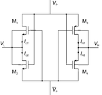
I'm designing a MOS Rectifier for a RFID like application. I'm about to test some different structures, first of all the four transistor cell. I'm using cadence virtuoso for simulations. The goal is to load the load capacitance Cl with the rectifier. The rectifier gets the input signal over an inductive coupling. You can see my testcircuit in the picture. My input frequency is 13.56MHz, the RLC networks should have this resonant frequency. Vp and Vp- are the differential inputs of my rectifier. Vl is my low output, Vh is my high output.

The problem I'm facing right now is that I get a lot of errors when I'm trying to simulate the circuit. When I'm simulating with a small load capacitance (1pF) it seems to work (transient to 1ms) ok, but if I increase the capacitance (goal is about 1uF) I get a lots of errors. They all seem to be convergence errors or zero diagonales found in the jacobian at Vp. I don't really now where this problem comes from.
The thing I'm not shure about is where I have to put the ground terminals. I have one in the source circuit, but I don't think I should use one in the circuit of my transponder, since this would be equal to a direct connection from my source to my transponder(?).
I hope you can help me out.
Greetings, Harry
I'm designing a MOS Rectifier for a RFID like application. I'm about to test some different structures, first of all the four transistor cell. I'm using cadence virtuoso for simulations. The goal is to load the load capacitance Cl with the rectifier. The rectifier gets the input signal over an inductive coupling. You can see my testcircuit in the picture. My input frequency is 13.56MHz, the RLC networks should have this resonant frequency. Vp and Vp- are the differential inputs of my rectifier. Vl is my low output, Vh is my high output.

The problem I'm facing right now is that I get a lot of errors when I'm trying to simulate the circuit. When I'm simulating with a small load capacitance (1pF) it seems to work (transient to 1ms) ok, but if I increase the capacitance (goal is about 1uF) I get a lots of errors. They all seem to be convergence errors or zero diagonales found in the jacobian at Vp. I don't really now where this problem comes from.
The thing I'm not shure about is where I have to put the ground terminals. I have one in the source circuit, but I don't think I should use one in the circuit of my transponder, since this would be equal to a direct connection from my source to my transponder(?).
I hope you can help me out.
Greetings, Harry
