Continue to Site

Welcome to EDAboard.com

Welcome to our site! EDAboard.com is an international Electronics Discussion Forum focused on EDA software, circuits, schematics, books, theory, papers, asic, pld, 8051, DSP, Network, RF, Analog Design, PCB, Service Manuals... and a whole lot more! To participate you need to register. Registration is free. Click here to register now.

mos-bipolar pseudoresistor

Status
Not open for further replies.

mohamadzi

Junior Member level 1
Joined
Jan 12, 2013
Messages
17
Helped
0
Reputation
0
Reaction score
0
Trophy points
1,281
Visit site
Activity points
1,395
hello
I want to simulate
Reid Harrison paper "A Low-Power Low-Noise CMOS Amplifier for Neural Recording Applications" that he is using a mos-bipolar transistor to implement such similar pseudoresistor.
Does anyone has the technology files of this mos-bipolar?
I search in mosis.com but I couldn’t found any file about this.
 

... a mos-bipolar transistor to implement such similar pseudoresistor.
Does anyone has the technology files of this mos-bipolar?

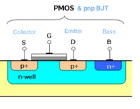
I think you can't get nor need a technology file for that; together with Fig.1 (p. 1) and the description in item A. (p.2) it's sufficiently explained: it's simply a 4µm*4µm pMOSFET, G connected to D , and S connected to Bulk, which acts as a pnp BJT if VGS is positive and so puts the pMOS into off region. Then G=D is positive against the source, hence the D becomes the emitter of the pnp BJT, the source becomes the collector, collector and base are connected, s. the foll. image:
In both functionalities (MOS & BJT), at sufficiently small VGS (≦ |0.2V|) they act as a pseudoresistor, s. Fig.3.

For schematic simulation you must instance both the pMOS and the pnp BJT for each device.

Note: In layout you need separate n-wells for each transistor Ma .. Md.
 
For schematic simulation you must instance both the pMOS and the pnp BJT for each device.
.
thank you
but i have a question
for simulate mos-bipolar i must be pmos and pnp in series?
 

for simulate mos-bipolar it must be pmos and pnp in series?
No, in parallel of course. Connect them as shown in the image above: emitter to drain, base to bulk, collector to source. Then connect C=S to B, and G to D. Separately for each Ma .. Md.

For the pnp BJT, use the lateral one (medium current gain), if available.
 
i try to simulate it bur i cant:-(
can u help me more plz...
 

Status
Not open for further replies.

Similar threads

Part and Inventory Search

Welcome to EDABoard.com

Sponsor

Back
Top