engrvivs
Junior Member level 3
Hi,
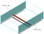
This is related to layout design in Agilent's ADS-2008 (or 2009) for EMDS simulation. I want to know if the port area, as shown by EMDS > 3D EM Preview, can be modified by the designer? By port area, I mean the port boundaries, depicted as shaded portions in figure below:

I found that ADS software automatically sets the port areas as follows:
ADS-2008 Wp = 07 x Wstrip Hp = 04 x Hsbstrt
ADS-2009 Wp = 21 x Wstrip Hp = 11 x Hsbstrt
where,
Wp and Hp => the width and the height of the port area, respectively;
Wstrip => width of the microstrip line
Hsbstrt => height of the substrate
Moreover, it would also be beneficial if someone can suggest appropriate port dimensions for correct simulations in any FEM software. I found that HFSS tutorial suggests Wp = 20 x Wstrip and Hp = 15 x Hsbstrt.
Thanks in Advance,
Vivs
This is related to layout design in Agilent's ADS-2008 (or 2009) for EMDS simulation. I want to know if the port area, as shown by EMDS > 3D EM Preview, can be modified by the designer? By port area, I mean the port boundaries, depicted as shaded portions in figure below:
I found that ADS software automatically sets the port areas as follows:
ADS-2008 Wp = 07 x Wstrip Hp = 04 x Hsbstrt
ADS-2009 Wp = 21 x Wstrip Hp = 11 x Hsbstrt
where,
Wp and Hp => the width and the height of the port area, respectively;
Wstrip => width of the microstrip line
Hsbstrt => height of the substrate
Moreover, it would also be beneficial if someone can suggest appropriate port dimensions for correct simulations in any FEM software. I found that HFSS tutorial suggests Wp = 20 x Wstrip and Hp = 15 x Hsbstrt.
Thanks in Advance,
Vivs