Continue to Site

Welcome to EDAboard.com

Welcome to our site! EDAboard.com is an international Electronics Discussion Forum focused on EDA software, circuits, schematics, books, theory, papers, asic, pld, 8051, DSP, Network, RF, Analog Design, PCB, Service Manuals... and a whole lot more! To participate you need to register. Registration is free. Click here to register now.

MMWave Layout Issues in CMOS

Status
Not open for further replies.

Puppet123

Full Member level 6
Joined
Apr 26, 2017
Messages
356
Helped
22
Reputation
44
Reaction score
21
Trophy points
18
Activity points
3,059
Hello,

I have designed a 3 stage amplifier at about 40GHz in CMOS.

I have done the layout using this methodology:

1) Layout Each Stage and then do RC extraction

-If interconnect is in DC path, ignore it

2) Connect them together using interconnect in Layout

3) I mimic the interconnect in schematic

Now some process kits, like IBM/Globalfoundries there is a TLINE component and a singlewire component.

I use the singlewire component in the schematic to see what effect the interconnect has on my design between stages in the RF path.

Or I could EM simulate all the interconnect lengths.

4) I use the TLINE component in layout for the interconnect I just simulated in the schematic.

Is this a proper methodology ?

Also, what the minimum interconnect length at a certain frequency before I have to EM simulate it ? At 30 GHz and below "can I get away with" not EM simulating the interconnect ?

Thanks.
 

At 40GHz you had better have a handle on L - RC only,
will lie to you big time. Known good tline structures are
nice, until you realize the cost of making everything on
the lineup a 50-ohm system (mucho power waste, large
layout and keep-aways, much bigger than desirable
devices, etc.).

For EM simulations you need the neighbors in place
and meshes can get real big real fast (with quite
opposite solution time and odds of finishing at all).

Probably not much use in a less than wavelength
tline but I'd defer to any expert on that.
 

Dick_FreeBird,

Thanks for your message.

The only way of getting a handle of the L as you said, is to do EM simulation of the passives and interconnect you feel are part of critical nodes in your circuit topology, correct ?

I mean you cannot - just not time for all that - just EM simulate all the interconnect between stages and all the interconnect at the inputs and outputs, unless they are critical - correct ? Too time consuming I would imagine.

Say I lay out one stage of a 3 stage MMWave amplifier - I extract the transistors and the interconnect. I am extracting one stage at a time to see the effect on the performance than using the extraction in simulation with the rest of non layout extracted stages to see how the performance changes. I deem the input node of my stage to be a critical node. If I EM simulate just the input node and associated passives, then use that to see the effect on performance, is that "more valid" than the RC extraction itself ? Do you understand my question ? Is their a purpose to doing an RC extraction and then EM simulation ?

Thank you.
 

Extract the active devices from your layout and leave passive components such as Transmission Lines, Coils,MiM Capacitors etc. then do your EM simulations with properly placed ports for each active element after that combine it with active elements in a schematic view ( Co-Simulation ).
This is very generic procedure for mmWave Integrated Circuits.
 

"properly placed ports for each active element after that combine it with active elements in a schematic view ( Co-Simulation ).
This is very generic procedure for mmWave Integrated Circuits."

Did you mean ""properly placed ports for each active element after that combine it with PASSIVE elements in a schematic view" ??
 

Did you mean ""properly placed ports for each active element after that combine it with PASSIVE elements in a schematic view" ??
Distributed Passive elements ( coils,transmission lines,mim caps. etc) will already be characterized by EM simulation,so you don't need to place them in schematic view.If there are lumped elements, you can also extract them from layout and place appropriate ports for them.After that, you should place either equivalent circuit or s-parameters defined instead of lumped components.
 

BigBoss,

Thank you for your response.

I have questions about how to define the ground plane.

I have attached some example layouts.

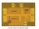
In one example there is a ground plane, I assume this is a "mesh" ground plane, popular in mmwave layouts. (the attachment that says Figure 6.6 - 60GHz amplifier)

In the other example I have drawn in crudely the connection to the ground pads. The reason is - I am wondering if these pads have to be connected to one another using a transmission line, of 50ohm, says in a top metal for lower loss. Then I can ground the inductors and the active devices in say metal 1 ground and then bring them up to that ground line in a top metal for lower loss. Can this line travel over the active and passive devices if in a higher metal.

I hope my questions are clear. I am trying to figure out how ground planes work in the layouts.

AmpGround.png60StageAmplifier.jpg
 

i don't know that is meshed ground but it may also be "tiling" at higher level.Tiling increases the stress resistance of the dies.I cannot say anything..
If N+1 metal layer traverse over on another metal layer/active layer there will absolutely be interaction between them.But since I don't know the foundry which you've been using, how much this interaction will be ??If I were you, I prevent to traverse anything over active devices (also passive devices) because the proximity effect may make crappy everything..
 

Thank you BigBoss.

Do the left and right gnd pads in the attachment I posted needs to be connected by interconnect - metal ?

I am confused as to what the "ground plane" is.
 

Thank you BigBoss.

Do the left and right gnd pads in the attachment I posted needs to be connected by interconnect - metal ?

I am confused as to what the "ground plane" is.

Ground Plane is the Plated Back Plane in MMIC technology.All GND connections are tied to this Back-plane through VIAS.
In other words, it is taken part of Opposite Side of the die..( glued to the die-pad).
 

Ground Plane is the Plated Back Plane in MMIC technology.All GND connections are tied to this Back-plane through VIAS.
In other words, it is taken part of Opposite Side of the die..( glued to the die-pad).

That's true for GaAs and other isolating III-V materials. The thread title says CMOS, and then indeed metal 1 layer would be a typical ground plane location, if microstrip is used at all.
 

What is the best resource (book, thesis, paper) for mmwave CMOS layout for optical / wireless ?
 

Status
Not open for further replies.

Part and Inventory Search

Welcome to EDABoard.com

Sponsor

Back
Top