David_
Advanced Member level 2
Hello.
I have a more or less complete design for a lab supply which I have been trying to implement on a 4-layer PCB, even if changes may occur this thread wont loose any value for my progress since they will if any minor.
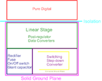
Here is a muck-up of the design to be the subject here:

This is my first such a complex PCB design and I am in many ways clueless about what might be the better or more correct layout to maximize performens, first of all we have:
Layer 1- top.
Layer 2.
Layer 3.
Layer 4- bottom.
The idea that I have gone with in this project is to have in the end two identical floating channels controlled by one and the same isolated µC, but I have begun to wonder if it would not be more suitable to have one small µC within the isolation area of each channel and perhaps communicate with those to a third small isolated µC that manages user interface and sends directions to the other two.
I will use some sort of AVR(95% sure of that since I am a hack at programming and AVR with the easy arduino solution will suffice for this time), they have tiny cheap µC's available.
That would be cheaper than to isolate SPI with multiple chip select lines as well as a handful of other signals needed, but the isolation was in part meant to isolate digital noise but with proper layout I now think that it could be fine without full isolation to digital circuits.
That's brings me to the next point, no matter µC isolation I still have SPI signals going into the analog parts of the board, my first layout went like this:

with the layers used as:
Layer 1- components
Layer 2. solid ground plane(in pink in picture)
Layer 3. digital ground plane
Layer 4- digital signals(as well as a couple of other tracks but not in any close proximity to digital)
I think my digital/analog stack-up might be flawed depending on how I connect them, but I want to ask about another concept.
What about if i keep it as I have just spelled out but move all data converters to the bottom plane only to via in right where i need them, they would be directly beneath the analog parts but with two ground planes in between?
Now I remember that I had hoped to fit some low voltage stuff on the third or fourth plane as well.
And what about putting a µC on the bottom plane as well though on a separate part of the PCB not directly under any analog circuits?
Then instead of massive digital isolators I could use a single SOIC8 I2C isolator to connect with the isolated control µC.
I guess what I am asking is: do you think I can keep so much digital so close the the analog output stage and still have a clean nice output?
I wish I had the economy not to ask and talk about it and simply learn by doing but I can't afford such a approach, though I think that talking about it with others is the right approach but learn by doing is as well the right approach. doing both would then be the best.
When I have found a solution that feels good I will order 5 boards and see how it went.
Any and all inputs are most welcome, I am about to start a carrier in electronics and I have not jet made up my mind if I want to try and approach the board layout part of electronics or the circuit design part.
As I understand it they are two different occupations?
Although the decision of where and with what I will endeavor my self to working with the next few years will be determined by what job I happen to find, as long as its in electronics it will be fine but why not have goals of where one want to end up one day.
Regards
David_
I have a more or less complete design for a lab supply which I have been trying to implement on a 4-layer PCB, even if changes may occur this thread wont loose any value for my progress since they will if any minor.
Here is a muck-up of the design to be the subject here:

This is my first such a complex PCB design and I am in many ways clueless about what might be the better or more correct layout to maximize performens, first of all we have:
Layer 1- top.
Layer 2.
Layer 3.
Layer 4- bottom.
The idea that I have gone with in this project is to have in the end two identical floating channels controlled by one and the same isolated µC, but I have begun to wonder if it would not be more suitable to have one small µC within the isolation area of each channel and perhaps communicate with those to a third small isolated µC that manages user interface and sends directions to the other two.
I will use some sort of AVR(95% sure of that since I am a hack at programming and AVR with the easy arduino solution will suffice for this time), they have tiny cheap µC's available.
That would be cheaper than to isolate SPI with multiple chip select lines as well as a handful of other signals needed, but the isolation was in part meant to isolate digital noise but with proper layout I now think that it could be fine without full isolation to digital circuits.
That's brings me to the next point, no matter µC isolation I still have SPI signals going into the analog parts of the board, my first layout went like this:

with the layers used as:
Layer 1- components
Layer 2. solid ground plane(in pink in picture)
Layer 3. digital ground plane
Layer 4- digital signals(as well as a couple of other tracks but not in any close proximity to digital)
I think my digital/analog stack-up might be flawed depending on how I connect them, but I want to ask about another concept.
What about if i keep it as I have just spelled out but move all data converters to the bottom plane only to via in right where i need them, they would be directly beneath the analog parts but with two ground planes in between?
Now I remember that I had hoped to fit some low voltage stuff on the third or fourth plane as well.
And what about putting a µC on the bottom plane as well though on a separate part of the PCB not directly under any analog circuits?
Then instead of massive digital isolators I could use a single SOIC8 I2C isolator to connect with the isolated control µC.
I guess what I am asking is: do you think I can keep so much digital so close the the analog output stage and still have a clean nice output?
I wish I had the economy not to ask and talk about it and simply learn by doing but I can't afford such a approach, though I think that talking about it with others is the right approach but learn by doing is as well the right approach. doing both would then be the best.
When I have found a solution that feels good I will order 5 boards and see how it went.
Any and all inputs are most welcome, I am about to start a carrier in electronics and I have not jet made up my mind if I want to try and approach the board layout part of electronics or the circuit design part.
As I understand it they are two different occupations?
Although the decision of where and with what I will endeavor my self to working with the next few years will be determined by what job I happen to find, as long as its in electronics it will be fine but why not have goals of where one want to end up one day.
Regards
David_