Continue to Site

Welcome to EDAboard.com

Welcome to our site! EDAboard.com is an international Electronics Discussion Forum focused on EDA software, circuits, schematics, books, theory, papers, asic, pld, 8051, DSP, Network, RF, Analog Design, PCB, Service Manuals... and a whole lot more! To participate you need to register. Registration is free. Click here to register now.

[SOLVED] minimum supply voltage

Status
Not open for further replies.

m_kuty

Member level 2
Joined
Mar 2, 2015
Messages
46
Helped
1
Reputation
2
Reaction score
1
Trophy points
8
Activity points
333
Hi everyone

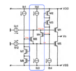
from textbook, the schismatic as attached is class-ab, and mention the minimum supply voltage. what dose mean that, and which transistor referring by

The minimum supply voltage of the output stage equals two stacked gate-source voltages and one saturation voltage, which makes it suitable for low-voltage operation.
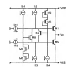
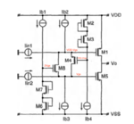
class-ab.PNG
 

I think the branches left of the output stage need at least three stacked gate-source voltages.
 

what is the minimum voltage range given?
 

To generate Ibias4 for example the bottom current source needs a Vdsat to operate, and top stacked M2 and M3 MOS diodes need 1-1 Vgs to be opened. Vgs is bigger than Vdsat, so else branches cannot determine minimum VDD like the middle transistors branch or the output stage, so it is really 2Vgs+Vdsat. I think.
 

... so else branches cannot determine minimum VDD like the middle transistors branch or the output stage, so it is really 2Vgs+Vdsat. I think.

In the middle branch (Ib2 & Ib3), M4 || M8 need at least 2Vgs to open M1 & M5 to allow operation in class AB output. Then at least 2 saturation voltages are needed for Ib2 & Ib3. This would make 2Vgs +2Vdsat for min. op. voltage.

Not sure - I'm neither J. Aaron nor Alan Bean :lol:
 

Yeah, I am not either, but if M4 and M8 is parallel then they will need 1Vgs I think, not 2Vgs. The output stage is 2 common-source amplifier, not 2 common-drain transistors. It doesn't require 2Vgs between the gates.
To guarantee that M1 is opened a bit for class-AB operation at the source of M4 (and at the drain of M8) it needs a VDD-Vgs voltage. For that and for the biasing of M4 then at the gate of M4 the voltage is VDD-2Vgs by the stacked diodes, M2 and M3. Same is implemented to open a bit M5, this is how it works.
I don't like when connections are not marked obviously with a simple dot, I won't understand why people draw it like this.
 

Yeah, I am not either
Right, Ference, maybe we both didn't find the right SCE switch! :-?

but if M4 and M8 is parallel then they will need 1Vgs I think, not 2Vgs.
Even less: I anticipate just 1*Vdsat

The output stage is 2 common-source amplifier, not 2 common-drain transistors. It doesn't require 2Vgs between the gates.
Right! I admit I've overlooked this :oops:

To guarantee that M1 is opened a bit for class-AB operation at the source of M4 (and at the drain of M8) it needs a VDD-Vgs voltage. For that and for the biasing of M4 then at the gate of M4 the voltage is VDD-2Vgs by the stacked diodes, M2 and M3. Same is implemented to open a bit M5, this is how it works.
Right. But now I made a new calculation - see this enlarged schematic pls.:
class-AB-output_1.png
Code:
VDD[SUB]min[/SUB]-Vgs = Vgs + Vdsat
Vdd[SUB]min[/SUB] = 2*Vgs + Vdsat
Tell me what you think, pls!

I don't like when connections are not marked obviously with a simple dot, I won't understand why people draw it like this.
Yeah, my opinion. That's why I provided the dots.
 

Thank you for all you reply,

You mention, Vgs and Vdsat, and these voltage should referring for transistor for taken account. pls can you be more precise. to understand the entire circuit.
 

Right, Ference, maybe we both didn't find the right SCE switch! :-?
Creepy erikl... :)
VDDmin-Vgs = Vgs + Vdsat
I don't understand why is it true, could you point the devices which are related? (index numbers of devices)

m_kuty, from my understanding the more precise value of Vdd.min = max(Vsg.2+Vsg.3+Vdsat.Ib4 , Vgs.6+Vgs.7+Vdsat.Ib1) ~ max(3*Vdsat+2*Vth.nmos , 3*Vdsat+2*Vth.pmos)
Where Vdsat is chsosen by the designer (set by Width and Length), Vth (threshold voltage) is coming from the process kit.
 

Creepy erikl... :)
Don't worry: we manage that! :grin:

I don't understand why is it true, could you point the devices which are related? (index numbers of devices)

Check the Ib2-Ib3 branch:
class-AB-output_1.png
VDDmin-Vgs = Vgs + Vdsat

VDDmin-Vgs is the voltage at gate of M1 (because M1 needs this to operate in class-AB)
Vgs is the voltage at gate of M5 (same argument)
Vdsat is the min. op. voltage of M4 || M8
 
  • Like
Reactions: m_kuty

    m_kuty

    Points: 2
    Helpful Answer Positive Rating
Ohhh, nice observation! I agree with it. Thus,

Vdd.min = max(Vsg.2+Vsg.3+Vdsat.Ib4 , Vsg.1+Vdsat.M4/M8+Vgs.5, Vgs.6+Vgs.7+Vdsat.Ib1)

I suppose in a decent design the middle section's spare voltage can be the highest and other bias branches determine the Vdd.min rather, but not sure and definitely it is not excluded.
I assume that in the stacked diodes, M3 or M7 have a bit bigger Vth because of the bulk-effect. I know, they can get them own floating well, but regurarly designers like smaller and cheaper solutions (I have never been used floating pwell for an nmos, it is luxury).
 
  • Like
Reactions: m_kuty

    m_kuty

    Points: 2
    Helpful Answer Positive Rating
pls can you be more precise.
In which respect?

to understand the entire circuit.
M4 || M8 together with Ib2 & Ib3 and the voltage sources at the gates of M4 resp. M8 establish a floating voltage source between the gates of the output transistors. For more info, check this PDF:

- - - Updated - - -

I assume that in the stacked diodes, M3 or M7 have a bit bigger Vth because of the bulk-effect. I know, they can get them own floating well, but regurarly designers like smaller and cheaper solutions (I have never been used floating pwell for an nmos, it is luxury).

No luxury if you really need them! And in this case: what are these extra floating wells compared to the size of the output transistors for a decent power output?
 

Attachments

  • Monticelli_Class-AB_biasing_scheme.pdf
    90.3 KB · Views: 137
  • Like
Reactions: m_kuty

    m_kuty

    Points: 2
    Helpful Answer Positive Rating
Yes, a decent power output is much bigger, but your output stage compared to the chip size and to die size is nothing. If you are using an extra mask just because your output stage really needs it the whole chip and die will have a big extra cost. NMOS floating pwell is expensive because of extra mask, and if you are using PMOS floating nwells a lot those need extra guard-rings to prevent latch-up, which will increase layout size. So it is extra cost too. People don't like to pay more. Anyhow I know these are possible, but I was forced always to solve problems without these.
 
  • Like
Reactions: m_kuty

    m_kuty

    Points: 2
    Helpful Answer Positive Rating
My last high volume custom design - 0.18µm process, 9 years ago - used a triple well process anyway, because several of the design team (8 guys) - including myself - needed floating n- and p-wells. The cost difference compared to a plain vanilla CMOS process was peanuts, I was told.
 

Interesting. We also worked on 180nm, and we were warned to don't use pwell, it was banned. I worked on an ISM band radio, it was lower complexity I think, later on higher complexity chips, not on the critical high speed circuits, and only the digital core was inplemented in deep nwell. We couldn't use higher voltage devices with floating pwell, I don't know why then. And actually it didn't change on 65nm or 40nm. Probably you did something very special, I would say what we have done were boring commercial products.
Feel yourself lucky please you could use pwell, not all of IC designers can enjoy it. :)
 

Status
Not open for further replies.

Part and Inventory Search

Welcome to EDABoard.com

Sponsor

Back
Top