Continue to Site

Welcome to EDAboard.com

Welcome to our site! EDAboard.com is an international Electronics Discussion Forum focused on EDA software, circuits, schematics, books, theory, papers, asic, pld, 8051, DSP, Network, RF, Analog Design, PCB, Service Manuals... and a whole lot more! To participate you need to register. Registration is free. Click here to register now.

microvias in allegro 16.2

Status
Not open for further replies.

buenos

Advanced Member level 3
Joined
Oct 24, 2005
Messages
960
Helped
40
Reputation
82
Reaction score
24
Trophy points
1,298
Location
Florida, USA
Activity points
9,116
hi

1.
how to create a microvia in allegro? step-by-step, please
in the pad designer program, there is an option for "microvia", just it is not available, which means its gray, i can not enable it. why?
actually it says type=through and there is no option to change it to BB via. microvia would be a BB via, i think.

2.
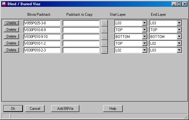
how to create a stacked via structure with 2 microvias from top to inner-1 and a big buried tht via from inner-1 to layer N-1. ?

which allegro documents describe this?
a few allegro pdfs talk about these, just they dont tell me where to click in the menus to do it.
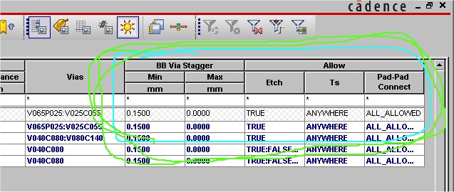
 

1)
A) Crate the via as a standard through via.
B)
This window shows how to setup vias as either blind or burried.


2) In constraint manager setup to use these new via types and set stacking to all allowed. Under analyse menu, choose modes, and look for the tap where stacking is mentioned, and set it 0 and 0 (min max).

PDF's ? Algroroute.pdf, in chapter 4.
 
thanks.

i cant really find the option for stacking allowed.
what is "0 and 0 (min max)" ? bb via stragger? what is it anyway?
 
I did a flaw, it was not under analyse and modes, but under physical - physical constraint set - all layers. out in the most outer right part.


max and min is center hole to center hole distance, as having vias stacked on top of each other, You should state nill = 0. Max distance ?? Hmm i don't know whats that is good for, but i allways state 0 :). for non stackted vias 0.3 should be set as min.
 

    buenos

    Points: 2
    Helpful Answer Positive Rating
hi

thanks.

is there an option to make 2 microvias to go to second layer, then one THT from there. or do i have to make the second microvia manually? for example power or gnd connection for a micro-BGA chip
 

imagine 10 layers.

Then You have a 0.1mm drilled and 0.3mm pad via, and a 0,25mm drilled and 0.6m pad via.

under setup - configure BB vias You make a Layer01-Layer02 via copied from microvia, then a Layer02-Layer03 also copied from microvia, now a Layer03-Layer08 copied from large via and equal from bottom side.

In the constraint manager You setup stacking for Your needs and for what the manufacturing farm demands.
 

i think you misunderstood me, or i misunderstand you.

what i wanted:

Code:
-----                        <-- SMT pad
V  V                        <-- 2 microvias
-----------
       I   I
       I   I                  <-- 1 THT via
       I   I
       I   I
       I   I
     -------

-
 

Status
Not open for further replies.

Part and Inventory Search

Welcome to EDABoard.com

Sponsor

Back
Top