rxb
Newbie level 5

- Joined
- Jul 16, 2014
- Messages
- 8
- Helped
- 0
- Reputation
- 0
- Reaction score
- 0
- Trophy points
- 1
- Activity points
- 99
Hello,
Let me preface this with saying I have no formal training in microwave transmission lines. Everything I know, which is not much, is self taught. I was tasked with creating a microstripline for the purposes of carrying a field in the 500 - 2000MHz range. Our goal is to use the lateral H-field produced by the line to drive small micromagnetic structures deposited on top of the line.
To design the line I've mostly relied on "Handbook of Microwave Integrated Circuits" by Reinmut K. Hoffmann and the design equations available in that book since I do not have access to an adequate EM simulation program. For impedance matching at 50ohms I used the equations by Hammerstad and Jensen. The line is very thin, only 100 nm of gold, so thickness corrections were insignificant. I am also not planning on going above 2GHz so dispersion did not seem like an issue either. I had to add two 90 degree bends which I mitered according to the specifications in that book. For the substrate I am using 0.5mm crystal sapphire. I also had to add a taper to reduce the width of the line to about 10um to get a strong enough H-field above the line. For the taper I followed paper "A Transmission Line Taper of Improved Design" by R. W. Klopfenstein. I made the taper as long as I could (1.5cm) to try and reduce the reflection at that low frequency I want to operate in.
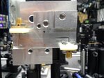
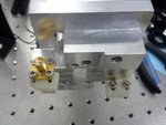
For the grounding plate we just used a large piece of aluminum on which the substrate and line sit. For the connections we used these sma to tab launchers found here
https://www.digikey.com/product-search/en?x=20&y=25&lang=en&site=us&KeyWords=A99392-ND
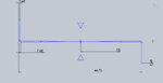
The connection is made via an insulating tab which applies pressure between the tab conductor and end of the line. I've attached a few images of the whole structure. I've also attached a sketch of the transmission line design and its dimensions.
To test the line I only have available an RF signal generator and a spectrum analyzer along with basic electronic components. I did a simple test to check the transmission by terminating one end directly into the signal generator and the other into the spectrum analyzer, both of which have 50 ohm terminations. Only about 25% of the signal amplitude was getting through the analyzer, so there are significant losses.
I have a few concerns. First due to the small dimensions of the center region with a cross section of 10um wide by 100nm thick the total dc resistance of the line is about 140 ohms. If I am not mistaken all of the design calculations assume that R << ωL. If the total inductance of the line is a couple of hundred nH then that is certainly not true in the 500-2000MHz range, so does that mean the impedance is off? I know at higher frequencies the current will tend to stick to the walls of the conductor due to the skin effect resulting in an increase of the resistance. From what I've been able to gather the total resistance goes something like \[ R_{dc} + R_{ac} \sqrt{ f}\] where Rac is inversely proportional to the skin depth. So I am assuming my biggest issue at the moment is severe conductor loss?
I am also concerned about the grounding plate and the connections. Is is that sma to tab launcher good for impedance matching? From what I read it is better to make contact via pressure rather than solder?
I apologize for the lack of specific details. I am looking for any general advice and issues that you folks might notice with my design/setup.
Let me preface this with saying I have no formal training in microwave transmission lines. Everything I know, which is not much, is self taught. I was tasked with creating a microstripline for the purposes of carrying a field in the 500 - 2000MHz range. Our goal is to use the lateral H-field produced by the line to drive small micromagnetic structures deposited on top of the line.
To design the line I've mostly relied on "Handbook of Microwave Integrated Circuits" by Reinmut K. Hoffmann and the design equations available in that book since I do not have access to an adequate EM simulation program. For impedance matching at 50ohms I used the equations by Hammerstad and Jensen. The line is very thin, only 100 nm of gold, so thickness corrections were insignificant. I am also not planning on going above 2GHz so dispersion did not seem like an issue either. I had to add two 90 degree bends which I mitered according to the specifications in that book. For the substrate I am using 0.5mm crystal sapphire. I also had to add a taper to reduce the width of the line to about 10um to get a strong enough H-field above the line. For the taper I followed paper "A Transmission Line Taper of Improved Design" by R. W. Klopfenstein. I made the taper as long as I could (1.5cm) to try and reduce the reflection at that low frequency I want to operate in.
For the grounding plate we just used a large piece of aluminum on which the substrate and line sit. For the connections we used these sma to tab launchers found here
https://www.digikey.com/product-search/en?x=20&y=25&lang=en&site=us&KeyWords=A99392-ND
The connection is made via an insulating tab which applies pressure between the tab conductor and end of the line. I've attached a few images of the whole structure. I've also attached a sketch of the transmission line design and its dimensions.
To test the line I only have available an RF signal generator and a spectrum analyzer along with basic electronic components. I did a simple test to check the transmission by terminating one end directly into the signal generator and the other into the spectrum analyzer, both of which have 50 ohm terminations. Only about 25% of the signal amplitude was getting through the analyzer, so there are significant losses.
I have a few concerns. First due to the small dimensions of the center region with a cross section of 10um wide by 100nm thick the total dc resistance of the line is about 140 ohms. If I am not mistaken all of the design calculations assume that R << ωL. If the total inductance of the line is a couple of hundred nH then that is certainly not true in the 500-2000MHz range, so does that mean the impedance is off? I know at higher frequencies the current will tend to stick to the walls of the conductor due to the skin effect resulting in an increase of the resistance. From what I've been able to gather the total resistance goes something like \[ R_{dc} + R_{ac} \sqrt{ f}\] where Rac is inversely proportional to the skin depth. So I am assuming my biggest issue at the moment is severe conductor loss?
I am also concerned about the grounding plate and the connections. Is is that sma to tab launcher good for impedance matching? From what I read it is better to make contact via pressure rather than solder?
I apologize for the lack of specific details. I am looking for any general advice and issues that you folks might notice with my design/setup.
Attachments

Last edited: