Continue to Site

Welcome to EDAboard.com

Welcome to our site! EDAboard.com is an international Electronics Discussion Forum focused on EDA software, circuits, schematics, books, theory, papers, asic, pld, 8051, DSP, Network, RF, Analog Design, PCB, Service Manuals... and a whole lot more! To participate you need to register. Registration is free. Click here to register now.

[SOLVED] Microstrip - SMA connector, tapered ground plane

Status
Not open for further replies.

Tybi

Newbie level 5
Joined
Sep 1, 2021
Messages
8
Helped
0
Reputation
0
Reaction score
0
Trophy points
1
Activity points
58
Hello,
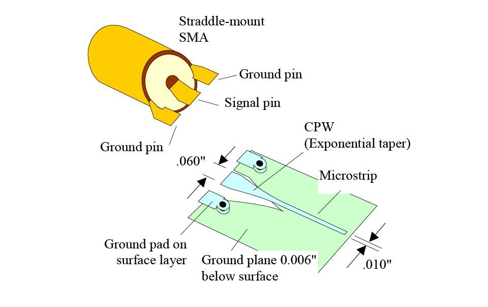
I'd like to have a transition from a SMA connector to a microstrip line with low reflection. I found a picture online with a tapered ground plane under the connector. But I can't find any reference to that picture. Has anyone tried this kind of structure? Or has somebody some literature recomandation for the sma to microstrip transition?

Regards
1630488586292.png
 

Assuming you got the diagram from http://www.sigcon.com/Pubs/edn/TaperedTransitions.htm there is a reference at the bottom of the page.
If I were designing a transition like that I would use an EM simulator as advised in the article, they have improved a lot over the 20 years since it was published. I would use a 3D simulator if you have one, though a good 2D type should get you close enough.
I've not tried 'defective ground plane' type transitions, but coplanar to microstrip with linear width change rather than exponential transition worked OK for me.
 

This is valid for particular SMA Connector.If you look at the Inner Pin, you'll see that the PIN is Larger than Ordinary SMA Connectors.Therefore, the Transition has been modified to avoid eventual Discontinuities at especially MicrowaveFrequencies.
 

Status
Not open for further replies.

Part and Inventory Search

Welcome to EDABoard.com

Sponsor

Back
Top