Continue to Site

Welcome to EDAboard.com

Welcome to our site! EDAboard.com is an international Electronics Discussion Forum focused on EDA software, circuits, schematics, books, theory, papers, asic, pld, 8051, DSP, Network, RF, Analog Design, PCB, Service Manuals... and a whole lot more! To participate you need to register. Registration is free. Click here to register now.

Microstrip balun design need help

Status
Not open for further replies.

TerryADS

Full Member level 2
Joined
Oct 31, 2008
Messages
133
Helped
2
Reputation
4
Reaction score
2
Trophy points
1,298
Location
USA
Activity points
2,066
microstrip balun

Hi friends,
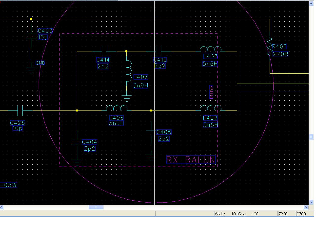
I want to invert 1.9GHz lump balun circuit in bellow schematic into microstrip balun in 5.5mmX5mm area,because we want to remove inductors for cost down.Anyone can kindly give me some tips about how to design it?
Thanks,
 

microstrip balun design

You can do it by using two components per path. but this may not assure the impedance matching on the balun side and also on required band with.

Current design has 4 components i.e 2nd order per path, which is very good to achieve the good performance.

I suggest to keep the same.
 

    TerryADS

    Points: 2
    Helpful Answer Positive Rating
lumped balun

The main reason for using lumped components is size, I guess. A straightforward microstrip solution can use a half-wave transmission line for phase reversal and possibly (for other designs than 1:2) a quarter-wave transformer for impedance matching - and require much more board space. As a small size alternative, multilayer chip baluns are available for 1.9 GHz, e.g. with 1:1, 1:2 and 1:4 impedance ratio.
 

    TerryADS

    Points: 2
    Helpful Answer Positive Rating
balun 1.9

Thanks.the main reason is size limitation and my boss requires us to remove the inductors for cost down.Balun circuit is connect to LNA,i need the balance port signals have the same amplitude and reveral phase(-90 and 90),Any topology i can select?
 

what is differential impedance for balun

For cost cut down, today inductors, tomorrow capacitors then entire balun?

Anyway forget it Boss is always right.

Try to realize these inductors using microstrip transmission line. I guess this is the only solution.
 

    TerryADS

    Points: 2
    Helpful Answer Positive Rating
1:2 balun design

need the balance port signals have the same amplitude and reveral phase
does this mean 1:4 (50 ohms single ended:200 ohms differential) impedance ratio? It could be achieved by just a 100 ohms impedance half-wave delay line in one port. You should clarify the impedance specification.

Regarding the Chipcon/TI application. Unfortunately, the application note doesn't distinguish between additional elements required to match the complex CC2430 output impedance (nominal 115 + j180Ω in the datasheet) and the balun as such. But it can give a rough estimation of the board space requirements. The delay line impedance has to be modified most likely.

the main reason is size limitation and my boss requires us to remove the inductors for cost down
Depending on board space costs, the replacement can decrease or increase the total costs. In some cases, additional space may be priceless. If you don't have free board space, you better stop the redesign immediately.

P.S.: A rough check gives an almost imaginary output impedance of your "balun" circuit at 1.9 GHz. It may be the case, that you don't know the specification at all?
 

    TerryADS

    Points: 2
    Helpful Answer Positive Rating
balun design ads

Terry
I know for sure that you're balun is feasible.

Some year ago, I've seen some realization of a mixed balun (some coupled line and a couple of capacitors) for DECT or Bluetooth.
There was a very small coupled line section iwht half-moon shaping, tuned by some capacitor, and it was in a working application.

But, I'm not able to find any reference about it, sorry.

Still trying...

Max

Added after 27 minutes:

I've got it!

Very nice, but requires tight tlerances in PCB process.


Max
 

    TerryADS

    Points: 2
    Helpful Answer Positive Rating
balun help

FvM said:
need the balance port signals have the same amplitude and reveral phase
does this mean 1:4 (50 ohms single ended:200 ohms differential) impedance ratio? It could be achieved by just a 100 ohms impedance half-wave delay line in one port. You should clarify the impedance specification.

Regarding the Chipcon/TI application. Unfortunately, the application note doesn't distinguish between additional elements required to match the complex CC2430 output impedance (nominal 115 + j180Ω in the datasheet) and the balun as such. But it can give a rough estimation of the board space requirements. The delay line impedance has to be modified most likely.

the main reason is size limitation and my boss requires us to remove the inductors for cost down
Depending on board space costs, the replacement can decrease or increase the total costs. In some cases, additional space may be priceless. If you don't have free board space, you better stop the redesign immediately.

P.S.: A rough check gives an almost imaginary output impedance of your "balun" circuit at 1.9 GHz. It may be the case, that you don't know the specification at all?
Sorry not to explain in detail.The balun is betwwen filter and LNA(integrated in MMIC).The balun is from 50 Ohm to 50 Ohm.Attached the datasheet for your reference.


Any documents I can supply so that you can give me more hand?
Thanks all for kind support,

Added after 2 minutes:


Hehe....Thanks vfone,Kspalla and Mazz.You are always kind to me.
 

50 ohms micro strip

I seems very unlikely, that the said RF19 transceiver has 50 ohms differential impedance. As already mentioned, the lumped "balun" has no real impedance, neither 50 nor 100 ohms.

The coupled microstrip solution in the paper presented by Mazz looks interesting because it's really small. But it's also rather high Q and requires precise PCB technology and exact tuning.
 

    TerryADS

    Points: 2
    Helpful Answer Positive Rating
balun micro strip

FvM

the lumped balun showed is common practice.

If you would like to check, just download and install the free AppCad software, that calculates automatically the 6 lumped elements balun starting from some R+JX differential impedance.

The basic idea is to shift signal of +90deg on one side and -90deg on other side, giving a symmetric structure.
Having 3 element per side, there is also the possibility to scale the impedance.

For example for 1.9 GHz and 50 Ohm differential, L=4.2 nH and C=1.7 pF.

Hope it can help.

Mazz
 

    TerryADS

    Points: 2
    Helpful Answer Positive Rating
~microstrip balun

Thank FvM for your reminder.I will make a measurement
 

micro-strip balun

the lumped balun showed is common practice
No doubt about it. I just mentioned, that in the shown dimensioning the output impedance is almost imaginary. You may want to designate any single ended to differential matching network a balun, so it's O.K. for the present one of course. At least you need an impedance specification.

It has been said, it should be 50:50 ohms, but it's very far from.
 

    TerryADS

    Points: 2
    Helpful Answer Positive Rating
microstrip delay line design

OK, now I've got it.

Terry maybe you forgot to mention the complete impedance: 50+jX.

Mazz
 

    TerryADS

    Points: 2
    Helpful Answer Positive Rating
chip balun application circuit

Oh..My mistake.Thank FvM and Mazz for mention
 

Status
Not open for further replies.

Similar threads

Part and Inventory Search

Welcome to EDABoard.com

Sponsor

Back
Top