Continue to Site

Welcome to EDAboard.com

Welcome to our site! EDAboard.com is an international Electronics Discussion Forum focused on EDA software, circuits, schematics, books, theory, papers, asic, pld, 8051, DSP, Network, RF, Analog Design, PCB, Service Manuals... and a whole lot more! To participate you need to register. Registration is free. Click here to register now.

Metal width variation in CMOS nano meter Process

Status
Not open for further replies.

020170

Full Member level 4
Joined
Jan 31, 2005
Messages
231
Helped
3
Reputation
6
Reaction score
1
Trophy points
1,298
Activity points
2,221
optical proximity correction

Hello

I have a question on metal width variation in CMOS Process, especially nano meter process

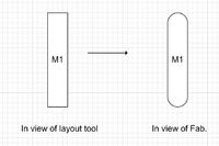
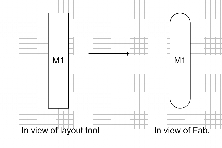
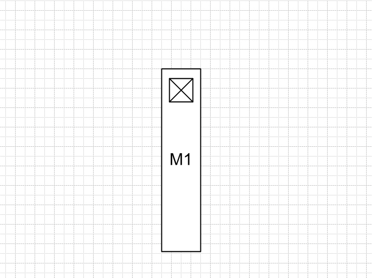
Metal line that I draw looks like square Line in layout tool. but in real metal line was not square line. it looks like rather round square line owing to etch processing. (see following Fig.)


In some case, Metal Line go round via or other metal line with minimum DRC rule. (see following Fig. metal line turns around other metal and via )


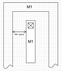
In this case, All metal width was reduced rather than the real size of metal width.

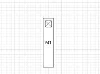
However, Only One Metal line was laid on some place, and there was no other metal near here, Metal width was increased rather than decreased by process variation. ( see following fig. no any other metal, this metal width is increased )


I witness this phenomenon today. but I don't explain why this phenomenon occur in very different way.

There is anyone who explain me in detail?

Thanks.
 

metal width length

Firstly it is not the metal etching that rounds off square corners. This is due to the camera that prints the layer prior to etching. The camera cannot completely resolve a square corner as it uses a finite wavelength which limits its resolution. To accurately image a square corner exactly would require infinite resolution.
So this is a fundamental limitation of optical physics. All corners will be rounded. This can be alleviated by using Optical Proximity Correction, where extra small squares are added to each corner like ears, which cause the optical image to appear squarer but not completely square.

Now where there are 3 or more lines of pattern at minimal spacing, the diffraction effect can cause the line(s) in the middle of the pattern to be reduced in width. Again this is a fundamental limitation of optical physics. Lines with no other pattern close by will not experience this reduction. Unfortunately you cannot compensate for this by increasing the width of dense (minimum spaced) structures in the centre as this will reduce the space, the camera will not adequately resolve the space leading to bridging shorts.

However, typically for metal etch process, isolated lines are reduced in width relative to dense lines due to the chemistry of the plasma etch and its polymerisation. This effect tends to compensate for the optical effect but not completely.

If isolated lines are wider than drawn, then this is probably due to the reticle biasing done by the fab. That is, every process using the camera to image the pattern, then etching of that pattern, will have an offset between initial imaged size and completed etch size. This will be known to the Fab and compensated by either increasing the drawn size on the reticle or decreasing it, such that final size is at, or close to drawn size at design. Now this cannot account for all process variations due to camera and etcher. so a compromise is reached.
For metal lines, it is better to have wider isolated lines than dense lines too thin due to electro-migration considerations and defects from too narrow lines such as opens or not fully surrounding Vias etc. So this compromise means that all lines are increased in size such that dense lines (affected by diffraction) never go below the minimum specification. This unfortunately means all isolated lines will be wider - but who cares?
 

Status
Not open for further replies.

Similar threads

Part and Inventory Search

Welcome to EDABoard.com

Sponsor

Back
Top