krishanu007
Member level 2
- Joined
- Apr 8, 2010
- Messages
- 49
- Helped
- 0
- Reputation
- 0
- Reaction score
- 0
- Trophy points
- 1,286
- Location
- Bangalore,India
- Activity points
- 1,594
hiii friends,
i am working on cadence virtuoso,on a ALU project.
Can u please explain or give links to any tutorial about..
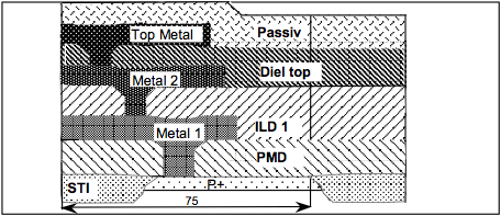
•difference of me1,me2
•how contact layers work
•what are n-wel,n-diff etc.???
pls i am in a bit hurry...
Added after 3 minutes:
i am beginner to cadence virtuoso.:?:
i am working on cadence virtuoso,on a ALU project.
Can u please explain or give links to any tutorial about..
•difference of me1,me2
•how contact layers work
•what are n-wel,n-diff etc.???
pls i am in a bit hurry...
Added after 3 minutes:
i am beginner to cadence virtuoso.:?: