ashourism
Newbie level 6

- Joined
- May 17, 2012
- Messages
- 12
- Helped
- 0
- Reputation
- 0
- Reaction score
- 0
- Trophy points
- 1,281
- Location
- Egypt
- Activity points
- 1,381
Hi
I am working on a Pipelined ADC
1. I have built an ideal system that gets an ENOB of 7.99
2. I created a Folded Cascode amplifier that settles in 3ns with GBW 200MHz and Gain 61dB and put it into the system then i got an ENOB of 7.8
but now i am trying to replace the DAC and the switches with real components however i am facing very strange issues and problems and i hope to know if someone can help me with it
I will try to be organized as much as possible and as informative as possible in this post so i apologize for its long size
General Notes
1. Supply Voltage = 2.5V
2. Common Mode level 1.2V
3. Vref = 1.5V
4. -Vref = 0.9V
5. Fsampling = 12.5MHz
6. Input signal is a differential sine wave of 600mV peak to peak and frequency 765KHz
7. All testing done here with an Ideal amplifier of GBW = 200MHz and very high gain
1. The Ideal MDAC Stage
#All blocks here are built using VerilogA and switches are Cadence built in Relays
##The Ideal Stage Schematic :
##The Ideal Stage Transient Response :
##The Ideal Stage Tran. Response Colour Code :
2. The DAC Circuit
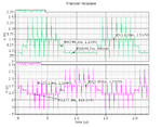
##Unloaded DAC Circuit Schematic and Its transient Response
->The DAC Circuit Schematic (with color code) :
->The Unloaded Transient Response :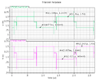
3. The DAC in MDAC Circuit with Switches
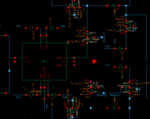
## The Non Ideal System Schematic :
## The Non Ideal System Transient Response :
## Response Color Code :
4. The DAC in MDAC Circuit with Switches with an attempt to correct DAC Output with a 2pF Cap
## Schematic: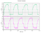
## Output :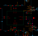
5. Effect of Correction on Whole Stage
## The Non Ideal System Transient Response (Corrected) :
## Response Color Code :
----------------------------------------------------------------
ENOB with switches and Non_Ideal DAC drops to 0.5! and signal output is distorted significantly, I really don't know where is the problem, i have tried all of the following
1. custom size for NMOS inside DAC and outside this has worked to get a neat DAC Stage and avoid clock feedthrough and charge injection
2. Using Transmission Gates
3. Using Transmission Gates with 1/2 W dummy transistor on both sides of the N and P Mosfets
4. I don't understand the cause of the glitches and i hope someone can help me with it?
Thanks
I am working on a Pipelined ADC
1. I have built an ideal system that gets an ENOB of 7.99
2. I created a Folded Cascode amplifier that settles in 3ns with GBW 200MHz and Gain 61dB and put it into the system then i got an ENOB of 7.8
but now i am trying to replace the DAC and the switches with real components however i am facing very strange issues and problems and i hope to know if someone can help me with it
I will try to be organized as much as possible and as informative as possible in this post so i apologize for its long size
General Notes
1. Supply Voltage = 2.5V
2. Common Mode level 1.2V
3. Vref = 1.5V
4. -Vref = 0.9V
5. Fsampling = 12.5MHz
6. Input signal is a differential sine wave of 600mV peak to peak and frequency 765KHz
7. All testing done here with an Ideal amplifier of GBW = 200MHz and very high gain
1. The Ideal MDAC Stage
#All blocks here are built using VerilogA and switches are Cadence built in Relays
##The Ideal Stage Schematic :

##The Ideal Stage Transient Response :

##The Ideal Stage Tran. Response Colour Code :

2. The DAC Circuit
##Unloaded DAC Circuit Schematic and Its transient Response
->The DAC Circuit Schematic (with color code) :

->The Unloaded Transient Response :

3. The DAC in MDAC Circuit with Switches
## The Non Ideal System Schematic :

## The Non Ideal System Transient Response :

## Response Color Code :

4. The DAC in MDAC Circuit with Switches with an attempt to correct DAC Output with a 2pF Cap
## Schematic:

## Output :

5. Effect of Correction on Whole Stage
## The Non Ideal System Transient Response (Corrected) :

## Response Color Code :

----------------------------------------------------------------
ENOB with switches and Non_Ideal DAC drops to 0.5! and signal output is distorted significantly, I really don't know where is the problem, i have tried all of the following
1. custom size for NMOS inside DAC and outside this has worked to get a neat DAC Stage and avoid clock feedthrough and charge injection
2. Using Transmission Gates
3. Using Transmission Gates with 1/2 W dummy transistor on both sides of the N and P Mosfets
4. I don't understand the cause of the glitches and i hope someone can help me with it?
Thanks
