Welcome to our site! EDAboard.com is an international Electronics Discussion Forum focused on EDA software, circuits, schematics, books, theory, papers, asic, pld, 8051, DSP, Network, RF, Analog Design, PCB, Service Manuals... and a whole lot more! To participate you need to register. Registration is free. Click here to register now.
Maximum input power for a GaN transistor is meningful only to not damage the transistor, and not for other paramaters as P1dB, which is an important parameter in LDMOS, BJTs, CMOS, or JFETs.
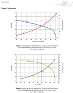
In GaN, if you look to the plots of gain vs output/input power, will see that GaN devices starts to compress at very low power levels, when other types compress right before saturation.
Maximum input power for a GaN transistor is meningful only to not damage the transistor, and not for other paramaters as P1dB, which is an important parameter in LDMOS, BJTs, CMOS, or JFETs.
In GaN, if you look to the plots of gain vs output/input power, will see that GaN devices starts to compress at very low power levels, when other types compress right before saturation.
Okay, you say that we can operate it well beyond P1dB, but what is the maximum input power(in dBm) for safe operation.
I found a research paper using ~31dBm (which I calculated by subtracting gain from the output power, they reported)
So I decided to move with 30dBm
Any suggestions
The plots shown are 42 dBm - 18db = 24 dBm input max. So 30 dBm (1mW) is a bit high but possibly safe for an input without considering output temp rise.
--- Updated ---
Considering this is a FET, there is not much power dissipated in Rg at 1mW input, which is primarily absorbed by the external 47 or 50 R resistor, so this irrelevant to consider a limit for safety of the resistor in an FET spec.
what is the maximum input power(in dBm) for safe operation.
I found a research paper using ~31dBm (which I calculated by subtracting gain from the output power, they reported)
So I decided to move with 30dBm
Any suggestions
There is no information in the datasheet about safe maximum input power for this transistor.
Only the manufacturer can give you this information.
In a design you can assume any maximum input power you want, but not when is about damaging the device. So, ask the manufacturer about this information..
There is no information in the datasheet about safe maximum input power for this transistor.
Only the manufacturer can give you this information.
In a design you can assume any maximum input power you want, but not when is about damaging the device. So, ask the manufacturer about this information..
This site uses cookies to help personalise content, tailor your experience and to keep you logged in if you register.
By continuing to use this site, you are consenting to our use of cookies.