Continue to Site

Welcome to EDAboard.com

Welcome to our site! EDAboard.com is an international Electronics Discussion Forum focused on EDA software, circuits, schematics, books, theory, papers, asic, pld, 8051, DSP, Network, RF, Analog Design, PCB, Service Manuals... and a whole lot more! To participate you need to register. Registration is free. Click here to register now.

MAX II CPLD & Quartus Issue

Status
Not open for further replies.

djh82uk

Newbie level 5
Joined
Feb 16, 2021
Messages
8
Helped
0
Reputation
0
Reaction score
0
Trophy points
1
Activity points
108
Hi Guys,

Im pretty new to CPLD's & FPGA's. I am a hobbyist with a background in IT. I am working towards building an 8-Bit computer.

Ive been following guides and have managed to get past most of my issues.

The issue I have now is this: I am following a schematic for a circuit that drives a test signal via VGA. The original used mostly 7400 series chips, so I figured I could copy that as a learning exercise. The only part of the circuit that used analogue components was the 555 with it's cap and resistors, so I figured out the timing it would have, and replicated that by building a clock divider from the boards Oscillator. I tested that on the board by itself and it was fine and confirmed the timings with a logic analyzer.

I then proceeded to build the rest of the design.

Now I am compiling without errors, but it says that it is going to use zero LE's. There are lots of warnings for "Warning (13027): Removed fan-outs from the following always-disabled I/O buffers" which im guessing is the reason why.

Now I may have been a bit stupid here, but as im using the block diagrams to build it, I wanted to build up the library myself (to learn, and get to grips with the tools), so I only used NAND2 and Tri gates from the Quartus library, and used those to build everything else, eventually ending up with a few 7400 series logic chips. (built from their datasheets)

The Tri's it's complaining about sit inside the 74244 IC's which output to the pins. Yet the Tri's are tied to an input, which is driven by another IC. I just can't figure out why it thinks the Tri's will always be tied to Ground (and therefore to ignore them)

Ive got everything here on github LINK, or can post the errors. The Github has the RTL view exported, and the source folder shows the original schematic. But I guess it's my implementation thats the issue.

Any advice would be greatly appreciated.
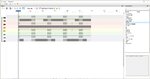
 

Modern FPGA have no internal tri-state drivers and must perform a translation during synthesis.

IMO you should not translate a 7400 series schematic into an FPGA design directly, that is not a useful learning experience (beside learn that you shouldn't do that). You should determine what the circuit does then implement it in an HDL (Verilog/VHDL), instead of a library of gate level primitives that are then used to create 7400 series blocks.
--- Updated ---

I see you are doing this as a schematic....ugh.

Scalability is an issue if you design using schematics of very small blocks building larger blocks. An 8-bit CPU will take 100's of 74374 flip-flops in the schematic to implement it. Imaging trying this with a >100k flip-flops in a modern 64-bit processor. You would have a schematic requires 1000's of pages.

Designing with a high level synthesis tool (C to gates) or using VHDL/Verilog is normally used to implement large designs.
 
Last edited:
Hi, Thanks for that

My intention was always to go the Verilog route, but it's taking me an amount of time to try and get to grips with it. I assumed that my method was in-efficient, but for now it was allowing me to achieve some level of success (but not with this one).

I will take on board what you said, and try to get further with Verilog. Maybe try the clock divider on it's own first.

I guess I am still curious as to why I may be having this issue though, the fact that the abstract of a tri-state exists indicates that there is a way for it to work?

I am working on the computer alongside this, using actual gates. Again, far from the most efficient method I know as previously I would have just done it on a micro. I was trying to get down into the weeds, and in doing so get a better understanding of the lower level stuff so that I know what im asking it to do.

I appreciate that this may not be "normal" but ive never been able to learn the normal way.

Thanks
 

Despite of the valuable comments by ads-ee, schematic entry is still a design description method supported by Quartus. Although rather uneffective, in can be used to implement FPGA designs.

The reported problems with your design are not primarily related to using schematic entry, rather inconsistent logic which can be created by any entry method.

I need to compile your design to see where the fault is.
--- Updated ---

As explained by ads-ee, internal tri-states are not real in FPGA or CPLD designs but emulated as muxes and typically generating a lot of synthesis warnings. But they work though.

According to the thread title, you want to implement a CPU on MAX II CPLD. I'd suggest to use a slightly more powerful device. MAX II is already discontinued, cost is a multiple of recent devices.
 
Last edited:
Ah yes, im currently just testing this design for pushing to a VGA display on the Max II. That was while waiting for my Cyclone IV to arrive (de0-nano), which it now has (took some saving).

I was kind of treating the Max II as a sacrificial lamb in case I mess up too badly while learning (As it cost around £7 for the board). I have no idea whether the VGA test design will fit, as it just says it is using up zero LE's when synthesizing. I kind of assumed it wouldn't as the clock divider alone took up 19% of it's 240 LE's

I do have a question on the Mux as Tri-State, how does it get the third state of "not connected"? Or is that also abstracted away?

Ive noticed I also have errors such as:
Warning (13024): Output pins are stuck at VCC or GND

And it calls out the two Hsync and the two Vsync pins, so all three sections of the design are doing something unintended. Those Sync pins are driven by a couple of And8 gates. So is it finding some scenario where they can never change state?

I get that it's more likely that Im the fault here, but is there a chance it's getting confused by something?
--- Updated ---

Ok, made some progress. I def messed up, where I had all the AND8 gates, they should have been NAND8. Changing them out got rid of the pins always tied to GND or VCC messages.

On the 245's, I still don't know what was wring, but swapping them out with the 245's that come with the Max ii device files/library sorted out the tri warnings. Not I have no real warning and it's taking up 100 or so LE's.

I don't have a scope or a VGA cable yet, but just putting the logic analyser on the output pins shows a nice pattern of transitions where there was nothing before.

I am keen to progress to Verilog, any advice on a good source for a real beginner? I did look at VHDL but it looks a lot more verbose and figured it would be harder to learn?

Thanks Both
 
Last edited:

The tutorial located here seems to be decent. It also uses Verilog 2001 (C-style) syntax for module ports, whereas many tutorials use the original verbose method of declaring the ports and then declaring the input or output direction separately (repeating the port names).

ASIC-world has a lot of information and a nice set of code examples for basic logic blocks.
 

FYI - using the built in graphical tools for low level design was considered "out of date" 15 years ago. It comes from a time when the circuit designers were also generating the FPGA logic and a lot of them liked the graphical interface. But as mentioned, it doesnt scale, isnt portable and doesnt work with version control.

As for which HDL - the choice of simply Verilog vs VHDL isnt quite the answer any more. C-to-gates is now well supported in Xilinx at least BUT... you really need a good understanding of hardware design to actually get meaningful results out of it, however they may sell it. Matlab has HDL coder. There is MyHDL in python. But again, all of these are mearly tools that generate HDL (Verilog or VHDL) in known patterns, so understanding one of these is usually very beneficial.

The Verilog vs VHDL wars have been raging for years. Verilog (Since 2005 Verilog is now a subset of SystemVerilog) is the language of choice for ASIC design, hence has a stranglehold in the states and India (as a lot of design houses have indian offices) with a lot of the verification being done in SystemVerilog. It has a lot of C-like syntax and can feel very comfortable for a software engineer, particularly if you are used to C/C++/Java (as classes in SV are based on Java).

On the flip side is VHDL. Based on ADA in the early 80s, it has a much lower adoption than Verilog with its used mostly confined to FPGAs but has a fairly strong use in Europe. Like @ads-ee points out for verilog, it also suffers from old text books and tutorials lingering around from years past. If you do decide to give VHDL a go, try and find a tutorial that at least mentions VHDL 2008. It appears to be getting a strong push from Aldec at the moment now a few open source verification libraries are mature, and a new standard, VHDL 2019 has been released.

I have seen it written that if you are an experienced C programmer, you should avoid verilog and go for VHDL. Because the language is so alien, you may be less likely to fall into software traps when writing in verilog. But at the end of the day, both VHDL and Verilog can do the same things. Its all about what you know.
 

Regarding your initial post, the design compiles apparently correct

1613568428658.png

Misses any timing specification
 

Thanks All, lots for me to take away there.

FvM, you may have grabbed it after my updated post where I said I fixed it (AND 8 and the 74-244 chips were the issue). I don't have the VGA monitor to test with yet, but the attatched analysis at least shows it doing something :). Its some sort of progress at least.

Id really like to get this finished, and then may use that as the design to try and implement via HDL directly.

I don't yet understand the timing specification, so something else for me to dig into.
 

Attachments

  • sigrock.JPG
    sigrock.JPG
    132.3 KB · Views: 135

Hi Guys, so I managed to get the version built with the block diagram to sort of work. I then found some VHDL code that did something similar and tested that. Ive since had a go at writing my own in verilog which ive now got working. Its a bit simpler as it only displays a red screen, but it's stable at least.

I just wanted to say thanks for the guidance, probably seems a bit noddy to you but im pretty pleased :0

My verilog is below in case anyone has an ideas on what I should have done better (best practice wise)

Code:
module vga    (clk50, v_sync, h_sync, red_signal,green_signal,blue_signal, video_en);

input clk50;

reg [10:0]h_cnt;
reg [10:0]v_cnt;
output reg h_sync;
output reg v_sync;
output reg red_signal;
output reg green_signal;
output reg blue_signal;
output video_en;
reg horizontal_en;
reg vertical_en;

    
always @(posedge clk50)
begin   
//--Reset Horizontal Counter
if (h_cnt == 11'b010000001111)
    h_cnt <= 11'b000000000000;
else
    h_cnt <= h_cnt + 1;
end           


always @(posedge clk50)
begin       
//--Vertical Sync
//--Reset Vertical Counter
if (v_cnt >= 11'b001010011001 && h_cnt >= 11'b010000001111)
    v_cnt <= 11'b000000000000;
else if (h_cnt == 11'b010000001111)
    v_cnt <= v_cnt + 1;
end


always @(posedge clk50)       
if (v_cnt >= 11'b000000000000 && v_cnt <= 11'b01100011111) begin
        red_signal <= 1'b1;
        green_signal <= 1'b0;
        blue_signal <= 1'b0;           
end


always @(posedge clk50)
begin       
if (h_cnt <= 11'b01111001111 && h_cnt >= 11'b01101010111)
    h_sync <= 0;
else
    h_sync <= 1;
end


//--Generate Vertical Sync
always @(posedge clk50)
begin
if (v_cnt <= 11'b01010000010 && v_cnt >= 11'b01001111100)
    v_sync <= 0;
else
    v_sync <= 1;
end


always @(posedge clk50)
begin       
//--Generate Horizontal Data
if (h_cnt <= 11'b01100011111)
    horizontal_en <= 1;
else
    horizontal_en <= 0;
end


always @(posedge clk50)
begin       
//--Generate Vertical Data
if (v_cnt <= 11'b01001010111)
    vertical_en <= 1;
else
    vertical_en <= 0;
end

assign video_en = vertical_en && horizontal_en;


endmodule
 

You want some input on best practices...

It is twenty years since Verilog 2001 was introduced and the redundant module port naming can be done away with.
Code:
module vga    (clk50, v_sync, h_sync, red_signal,green_signal,blue_signal, video_en);
reg [10:0]h_cnt;
reg [10:0]v_cnt;
output reg h_sync;
output reg v_sync;
...
In Verilog 2001 syntax
Code:
module vga (
  input         clk50,
  output reg    v_sync,
  output reg    h_sync,
  ...
);

I would use something other than binary representation for count comparison, human readable decimal or hexadecimal are both better choices than binary. At least if you insist on binary use an "_" between every 4-bits to make it easier to read the binary value.

Don't use logical operators (&&) when you want a bit-wise operations (&).
Code:
assign video_en = vertical_en && horizontal_en;

Other suggestions I would make are cosmetic formatting, my take on code is anything to make it easier to read and to maintain is good practice. I've spent decades having to use old code where people write code that is very difficult to read or maintain and this has nothing to do with the functionality of the code merely the use of cryptic naming such as a, b, c, d names for signals which give no meaning to their usage. Run on characters, i.e. having no whitespace if the statement doesn't require whitespace to be understood by the parser.
e.g. using this:
Code:
if(a<=18'b101101001101011010&&(l!=18'b10000100101011010||f))y<=n+1;
FYI, there is a mistake, if you can spot it!
as opposed to this:
Code:
if (some_count <= 18'd 185_178 && (another_count != 18'd 67_930 || ignore_67930)) output_signal <= Input_signal + 1;

Wouldn't you rather see the second code snippet than the first, if you had to maintain or use the code?

Even more important is commenting your code, formatting can be fixed no comments requires reverse engineering code, which wastes everyone's time.
Comments like this are useless as the code itself can be recognized as a counter that has a reset.
Code:
//--Reset Horizontal Counter

Say why the counter is needed
Code:
//The horizontal counter is used to do set both the vertical sync and the horizontal sync and rolls over at X pixels
 
Last edited:

Thanks for the pointers, that's really helpful. I do some work in dev now and again for my job (not FPGA / EE obv) and im really bad for not commenting code until the end, or if it's just for me. But yeah is something I should def do better.

I learned the hard way that using binary for the counters was not the most fun way to do it. I started that way so saw it through, but will change it to decimal.

On the port naming, I think I must have learnt from some really old examples (or other people with that bad practice), even while being aware that there was another way of doing it. I'll spend some time improving it I think before looking to expand it to do more than just push a solid colour to the screen.

Many Thanks
Most of the online tutorials for Verilog haven't seem to been updated for 15 years.

How about making color bars
https://en.wikipedia.org/wiki/SMPTE_color_bars

That should be a sufficient increase in difficulty from the current design to make it a good choice.
 

As shown, the design doesn't generate actual output on the RGB signals, just assigning fixed values
Code:
        red_signal <= 1'b1;
        green_signal <= 1'b0;
        blue_signal <= 1'b0;
I presume you started with sync generation and didn't yet write meaningful RGB patterns?
 

Yeah, absolutely, my intention was to break it down and prove I had the vsync and hsync working well before looking to incorporate the colour channels. My thinking was to next have a go at writing alternate colours per line, and then maybe alternate colours per pixel.

And then look at a resistor dac to increase the number of colours. But figured I would need to lift the output upto 5V first to give it the range.
 

Please remember that most of the time shall be spent in verification and code debug. Therefore, also learn the debug tools like SignalTap and LAI in Quartus. It will help a lot in the future.
 

Ah, ive been trying to figure out what is included in the free version and looking for guides on it. Ive done a bit of playing with modelsim, but nothing really when it's on the board. I now have a Cyclone IV so hoping It will have a bit more I can do with it.
 

Status
Not open for further replies.

Part and Inventory Search

Welcome to EDABoard.com

Sponsor

Back
Top