Continue to Site

Welcome to EDAboard.com

Welcome to our site! EDAboard.com is an international Electronics Discussion Forum focused on EDA software, circuits, schematics, books, theory, papers, asic, pld, 8051, DSP, Network, RF, Analog Design, PCB, Service Manuals... and a whole lot more! To participate you need to register. Registration is free. Click here to register now.

matching connector to microstrip question

yefj

Advanced Member level 4
Joined
Sep 12, 2019
Messages
1,195
Helped
1
Reputation
2
Reaction score
3
Trophy points
38
Activity points
7,217
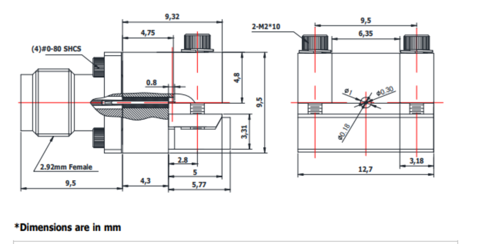
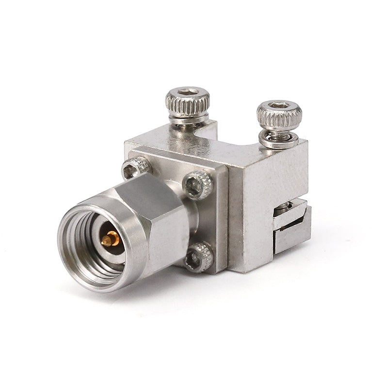
Hello I have a connector .we match 0.27mm microstrip trace to the connector using a taper.I know that a taper is transformer between impedances. given the connector shown below what kind of taper do you reccomend to build for proper transition of coax to microstrip?
Thanks.
1707070304880.png


1707071210549.png
 
If the pin length made any difference , you would see the effect at the f(1/4w) for 0.8 to 1mm range like at 100 to 80 GHz by some x dB ripple recursively.
Because the contact area is so small compared to the trace, I suggested the pin area (dia.*length) has less effect on impedance than the trace w/g under the pin.

We know sharp corners on traces changes flux density and has some EMC effects but I still wonder what affects the taper has vs none vs taper out towards edge.
 
Hello Klaus , i am trying to understand your words,currently i have only one cyilinder of 0.3mm sticking out 0.8mm
you say i need only 0.18mm cylinder sticking out at 0.762mm?
what about the 0.3mm cylinders,this is what gived me the 50Ohms.
so 0.3 is not sticking out at all?
i need to do tansition between 0.3 to 0.18mm?
Thanks.

1707389045100.png


1707390118784.png
 
Hello Volker, i have change the diameter of the sticking out part to 0.18mm.
i get -17db,what do you recoomend to change in order to get a better matching?
Thanks.
1707393867355.png

1707393920316.png


1707393899451.png
 
From what I can see in your plot, it is "var ref impedance" and not 50 Ohm S-parameters. So before you optimize something, make sure your ports are both 50 Ohm, and the resulting S-params are normalized to 50 Ohm.
 
View attachment 188443OD/ID=3.33 is correct.

The 0.18 mm pin has nothing to do with the interior impedance/dimensions.

1 mm and 0.3 mm has nothing to do with the PCB impedance.

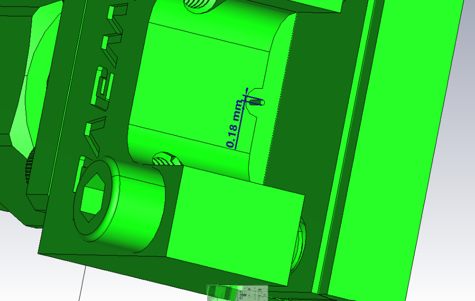
The pin over PCB on your selected connector is 0.18 mm D x 0.8 mm L.

It is this 0.18 mm circular shape that is pressed against the top layer #1 of your PCB as showed in my previous comment.

Your job is to match the edge feed impedance to the 0.18 mm pin and clamp ground return up < 18 GHz
I thought I was clear about not mixing internal and external dimensions.
Let me repeat with more clarity that the pin diameter and length is going to also be low sensitivity or irrelevant as the actual contact area with the trace amounts to a small area of a flat surface contacting a cylinder with < 0.1 Ohm conductivity expected. Now compared the air-gapped area of the remainder of the pin will amount << 1pF which is much higher impedance than the conduction path unless testing at 50 GHz well beyond the datasheet spec. This lead me to my conclusion that only the trace to ground controls the impedance. The reduced inductance of the contact area of the pin in parallel with the PCB trace will not significantly alter L/C ratio. (but my guestimate could be wrong) but a 1% change around -17dB RL is not much.

Unlike cheaper top soldered edge connectors, the amount of solder would affect s11 results above w/10 wavelength for the pin.

I suggest you replace the connector with a 50 ohm terminator to compare your s11 results. (or two 100 ohm terms to both sides of the ground plane)
 
Last edited:

LaTeX Commands Quick-Menu:

Similar threads

Part and Inventory Search

Welcome to EDABoard.com

Sponsor

Back
Top