Continue to Site

Welcome to EDAboard.com

Welcome to our site! EDAboard.com is an international Electronics Discussion Forum focused on EDA software, circuits, schematics, books, theory, papers, asic, pld, 8051, DSP, Network, RF, Analog Design, PCB, Service Manuals... and a whole lot more! To participate you need to register. Registration is free. Click here to register now.

LVS Error Report (Assura)

Status
Not open for further replies.

Kicchan

Member level 3
Joined
Feb 3, 2010
Messages
56
Helped
2
Reputation
4
Reaction score
2
Trophy points
1,288
Activity points
1,759
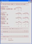
Can anyone help me in solving the LVS errors shown in the picture?
What are the Filter/Reduce Statistics?
Why does it return Unmatched Pins error? Moreover, I am not sure about the layers I used for pins and the corresponding labels. For example, input pin should be connected to metal1 so I chose ME1 (pn) for both the pin and the label "in". Is that correct?
 

Attachments

  • untitled3.JPG
    untitled3.JPG
    101.6 KB · Views: 132
Last edited:

The layer of the pin seems to be correct(highest layer used for the net), the text must be in the text layer(tt, etc.). Do check the direction of the pin in the layout and if it is attached and not floating. Filter Statistics is the devices that the tool recognizes if filter option is set. Look into Assura user guide for more.
Try to look into runname.cfr, .cls, .cps, .err files to understand the errors.
 
Thanks for your help, sulabh.
The direction of the nets are correct and I checked if any incomplete net is floating but everything seems to be ok...
I'll look through the files you suggested and see if I can find any clue...

---------- Post added at 16:06 ---------- Previous post was at 15:43 ----------

I checked the files you suggested.
Both .cfr and .err files are empty; .cps file contains only one commented line:
; autoPinSwap() results for schematic network.
The .err file is equal to the picture I have previously attached...
It follows that no new information is provided...
Any further suggestion? :cry:
 
Last edited:

Actually, the .cls file returns even the D G S B pins as unmatched pins both for the nmos and the pmos. Maybe it is not able to identify these pins. I've tried defining the mos pins in MosDevice within avCompareRules but it doesn't work...:cry:
 

you can compare the schematic netlist and the layout netlist for that, have you checked DRC before LVS
 
you can compare the schematic netlist and the layout netlist for that, have you checked DRC before LVS

My DRC is clean (with the exception of metal density but I think that's ok). I'll compare the netlists between schematic and layout then...Thank you
 

Status
Not open for further replies.

Part and Inventory Search

Welcome to EDABoard.com

Sponsor

Back
Top