Continue to Site

Welcome to EDAboard.com

Welcome to our site! EDAboard.com is an international Electronics Discussion Forum focused on EDA software, circuits, schematics, books, theory, papers, asic, pld, 8051, DSP, Network, RF, Analog Design, PCB, Service Manuals... and a whole lot more! To participate you need to register. Registration is free. Click here to register now.

[SOLVED] Lumped Port Slotline Simulation in HFSS

Status
Not open for further replies.

Zikloa

Newbie
Joined
Aug 5, 2020
Messages
3
Helped
0
Reputation
0
Reaction score
0
Trophy points
1
Activity points
34
Hi all, new user here. Hoping that I could find some help with simulating a slotline in HFSS. I've read many of the previous posts about this topic but they haven't been successful in helping me get a sensible simulation.

I think the main issue I'm having is positioning the lumped port. Where should this be placed on the substrate? How wide/tall should it be? Does it just need to touch each of the conductors? In any case, here's what I have right now:
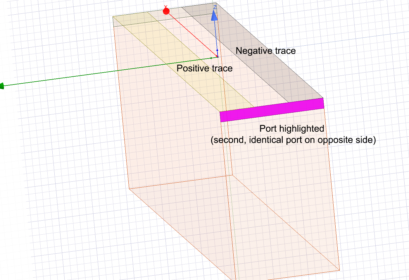
Ports.jpg


Also, is a lumped port on a driven terminal solution the best way to obtain the s-parameters for a slotline design, or should I be considering another simulation setup?

Any help would be greatly appreciated, TYIA.
 

Welcome, Zikloa.

Does your simulation setup have any other objects in it, other than what you've shown? There are numerous setup issues if that is all there is.

I find I get the best results using wave ports, but a lumped port should be ok. It should be placed between the two conductors (i.e., in the gap).
 
  • Like
Reactions: Zikloa

    Zikloa

    Points: 2
    Helpful Answer Positive Rating
Hey, thanks for getting back to me!

The only other object besides those pictured is a vacuum box containing the model. A radiation boundary has been applied to the faces of this box. Two other boundaries have been applied, those being PerfE boundaries on each of the conductors.

Regarding the port, when you say it should be in the gap, that means on top of the substrate? If so, is the only relevant dimension the width (to ensure that it touches both conductors), or does the length (along x axis) also play a role?
 

Regarding the port, when you say it should be in the gap, that means on top of the substrate?

Yes.

If so, is the only relevant dimension the width (to ensure that it touches both conductors)

Essentially, yes.

or does the length (along x axis) also play a role?

It will introduce some minor parasitics; there is no right answer, but I've found empirically that the best response seems to be from making the surface approximately square (length = width).
 
  • Like
Reactions: Zikloa

    Zikloa

    Points: 2
    Helpful Answer Positive Rating
Okay, makes sense. One last question: you said that you prefer to use a wave-port for this type of measurement, why?
 

Wave ports re-create the appropriate modal fields of only the desired mode, which is usually what your realistic excitation should be doing. The lumped ports will excite a spectrum of modes, which while realistic, is probably to a larger degree than you would typically find in a good excitation. Really, it's about modelling your real-world excitation to the best possible degree.
 
  • Like
Reactions: Zikloa

    Zikloa

    Points: 2
    Helpful Answer Positive Rating
Status
Not open for further replies.

Part and Inventory Search

Welcome to EDABoard.com

Sponsor

Back
Top