Continue to Site

Welcome to EDAboard.com

Welcome to our site! EDAboard.com is an international Electronics Discussion Forum focused on EDA software, circuits, schematics, books, theory, papers, asic, pld, 8051, DSP, Network, RF, Analog Design, PCB, Service Manuals... and a whole lot more! To participate you need to register. Registration is free. Click here to register now.

[SOLVED] LTSPICE Propagation delay calculation

Status
Not open for further replies.

Yukta2007

Junior Member level 3
Joined
Sep 13, 2020
Messages
30
Helped
1
Reputation
2
Reaction score
0
Trophy points
6
Activity points
156
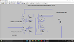
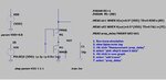
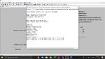
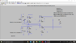
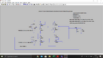
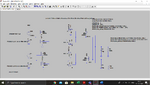
Could you please tell how to calculate propagation delay in LTSPICE for CMOS circuits.
Or is there any other software for calculation of delay of CMOS circuits?

Thank you.
 

Hi,

a rather general question.

So my general answer:
t_delay is from input voltage level xx to output voltage level yy.

The threshold level depend on: logic family, supply voltage, logic polarity.

Klaus
 

We are simulating this circuit in LTSPICE XVII and we are supposed to calculate the time delay for this circuit. Could you help us with that?
 

Attachments

  • 1.png
    1.png
    136 KB · Views: 1,042

I can´t tell.... but you should know where your input and output voltage threshold levels are.

Usually they are: V_IH, V_IL, V_OH, VOL.

Klaus
 

"calculate propagation delay in LTSPICE" doesn't make much sense. The delay can be measured in simulation waveforms, dragging the cursor or use a .measure statement. Or calculated with pencil and paper using simplified transistor models.

By the way, you keep posting flawed LTspice circuits, as in your previous thread. The nodes encircled in red have either unconnected wires or are shorting voltage sources. You should fix it to be sure what the simulated circuit actually is.

1602514186842.png
 

As I was going through the forum about how to calculate delay in ltspice I came across this answer which said how to calculate delay for an inverter circuit. Could u please explain me how the spice directive commands work here and also what does {RE} refer to here.
 

Attachments

  • Delay.JPG
    Delay.JPG
    140.2 KB · Views: 897

    adithyamc

    Points: 2
    Helpful Answer Positive Rating
Hi,
from post#2:
t_delay is from input voltage level xx to output voltage level yy.
see the 3 "MEAS" statements.
--> input level xx = 0.5 x VDD rising
--> output level yy = 0.5 x VDD falling
--> delay is the time inbetween

Klaus
 

"calculate propagation delay in LTSPICE" doesn't make much sense. The delay can be measured in simulation waveforms, dragging the cursor or use a .measure statement. Or calculated with pencil and paper using simplified transistor models.

By the way, you keep posting flawed LTspice circuits, as in your previous thread. The nodes encircled in red have either unconnected wires or are shorting voltage sources. You should fix it to be sure what the simulated circuit actually is.

View attachment 164722
Actually when we checked the error list, it shows no errors.
 

Actually when we checked the error list, it shows no errors.

In fact, a wire drawn over another wire is not an error; there is no way for the software to know our intent, you are the one who must ensure that the wiring diagram is drawn correctly.
 

Actually when we checked the error list, it shows no errors.
True, the horizontal wires running into the encircled transistor terminals are unconnected. But why did you draw it? To obfuscate the circuit function? You better delete it to avoid confusing others and yourself.
--- Updated ---

Circuit schematic without unconnected wires

1602603069107.png
 
Last edited:

True, the horizontal wires running into the encircled transistor terminals are unconnected. But why did you draw it? To obfuscate the circuit function? You better delete it to avoid confusing others and yourself.
--- Updated ---

Circuit schematic without unconnected wires

View attachment 164754
--- Updated ---

Circuit schematic without unconnected wires

View attachment 164754
Thank you. Will make these changes.
--- Updated ---

Hi,
from post#2:

see the 3 "MEAS" statements.
--> input level xx = 0.5 x VDD rising
--> output level yy = 0.5 x VDD falling
--> delay is the time inbetween

Klaus
Any idea about what does {RE} refer to? And why exactly is it needed here?
 

Hi,
Any idea about what does {RE} refer to? And why exactly is it needed here?
I never used it, but obviously
* RE = rising edge,
* FE = falling edge.

and you may use rising edge to falling edge (or vice versa) because you built an inverter.
Rising edge to rising edge won´t work.

Klaus
 

Hi,

I never used it, but obviously
* RE = rising edge,
* FE = falling edge.

and you may use rising edge to falling edge (or vice versa) because you built an inverter.
Rising edge to rising edge won´t work.

Klaus
Yes. I get that. But why is the value made to 1? Is there any particular reason? Or can it be taken at random?
 

Hi,

again. Never used it.
Did a 5 second internet search an found out that it`s the "1st" rising (or falling) edge.

So please try an internet search on your own. It´s not difficult.
I even assume your simulation tool has a "help". Use it.

Klaus
 

Yes. I get that. But why is the value made to 1? Is there any particular reason? Or can it be taken at random?
Why not use 2nd edge and check for differences? Despite of having powerfull .measure statements, it's usually faster and less error prone to read the delay with cursors from the waveform.
 

I have used the same .meas statements to calculate the propagation delay of my xnor circuit but the value is high(0.04s but we are supposed to get in ps) . I am attaching the files for reference.
 

Attachments

  • 2ref.png
    2ref.png
    162.7 KB · Views: 493
  • ref1.png
    ref1.png
    145.1 KB · Views: 398

Could you please help with the above query?
 

If it's not like expected... why don't you simply draw the waveforms?
As already twice recommended by FvM.

It's as simple as writing a new forum post.... and get immediate response..
Don't ignore the recommendation of an experienced member.

Klaus
 

Since there are very minute changes in our waveforms, calculation of delay using cursors on waveform is not possible. So we used .MEAS statements for calculating delay. Actually we have two circuits, one is basic xnor circuit and the other one is simultaneous circuit(the output of XOR and XNOR) should have the same delay.
We have 2 doubts:
1) The delay of simultaneous ckt is supposed to be same but we are getting different delay value(0.02 for XOR and 0.04for XNOR)
2) The delay of basic xnor circuit is also coming as 0.02
The project revolves about proving that simultaneous circuits are more efficient in terms of delay but we are unable to prove that. Could you please help?
I am attaching the screenshots for your reference.
 

Attachments

  • basic xnor.png
    basic xnor.png
    140.4 KB · Views: 294
  • simultaneous.png
    simultaneous.png
    153.2 KB · Views: 266

I don´t want to repeat the same again and again.

Thus I´m out. Good luck

Klaus
 

Status
Not open for further replies.

Part and Inventory Search

Welcome to EDABoard.com

Sponsor

Back
Top