Continue to Site

Welcome to EDAboard.com

Welcome to our site! EDAboard.com is an international Electronics Discussion Forum focused on EDA software, circuits, schematics, books, theory, papers, asic, pld, 8051, DSP, Network, RF, Analog Design, PCB, Service Manuals... and a whole lot more! To participate you need to register. Registration is free. Click here to register now.

LTC4020 battery charger charging current unstable

Status
Not open for further replies.

hoi

Newbie level 5
Joined
Oct 1, 2021
Messages
8
Helped
0
Reputation
0
Reaction score
0
Trophy points
1
Activity points
127
Hi everyone,

I am making a battery charger with LTC4020 to charge 12S li-lon battery but having problems for months and still could not fix it.

Input 24V
output 43V 2.5A charge current
battery voltage range 24V-43V (cell voltage 2V - 3.6V)
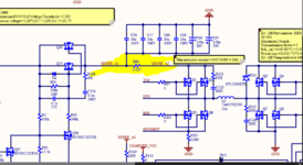
schematic setting
Maximum input current 10A
charging current 2.5A
battery float voltage 42.86V
Maximum output voltage 43.7V
Precharge voltage 28V

Problem
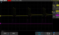
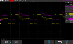
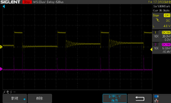
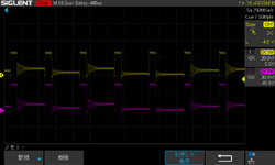
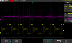
The charge current is lower than expected value, it should be maximum 2.5A but I could only get 0.5-1A charging current. And the waveform is strange.

I tried to tuned Vc and ITH value for weeks, it change a little bit with different value but could not solve the problem.

I tried to contact local FAE but did not get any useful information, tried to post the question in AnalogDevices forum but no one reply. Google searching LTC4020 and it seems some people here are using this chip so I think maybe I could get help from here. I would really appreciate if anyone could help.

The attachment is schematic, waveform of SW2 and charge current.

Thanks
 

Attachments

  • Charger_new.pdf
    615.1 KB · Views: 170
  • SDS00064.png
    SDS00064.png
    45 KB · Views: 170
Last edited:

Hi,

my hints:
* PCB layout problems
* inductor selection (saturation)
* capacitor selection
* maybe wiring

So if you show us details to the items above we can validate them.

Klaus
 
One pix does not tell the whole story .

Maybe 6 to 10 more with photo of measurement method of all the feedback and control signals and different load conditions. This could be a very high Q series resonant problem with good parts getting crosstalk or shootthru from improper deadtime or .... lack of damping from DNI

open circuit resonance is easiest to compute.
 
You posted a haystack and we're looking for a needle that is unable to regulate your charge current even if demand and supply exist. That means it getting false sensing signals or generating false demand current from noise. Validate your probe and layout methods by demonstrating a flatline on all your ground connections with adequate SNR..
 

Thanks so much the the replies!

Here is the details of the inductor.

Here is the layout and waveform
I tried to follow the evaluation board as much as possible.

All the waveform was captured in no load. I would take more if it could be helpful. Thanks
Sorry I only have 2 channel scope.

I use a DC power supply maximum 32V 10A, and set the input voltage to 24V during the test all time.
And I use a electric load to simulate the battery, I tried to connect to the battery but the perform was the same.

The inductor is very hot, 4 MOSFET are not that hot but still hot especially the 2 low side MOSFET.

Here is the efficiency I measured.

240.16320.290.0920.4771676892Precharge mode
240.16421.630.09351.10746951Precharge mode
240.16422.930.0940.5476168699Precharge mode
240.16522.580.0940.535989899Precharge mode
240.19127.190.1170.6939856021Precharge mode
240.19327.660.1190.7106088083Precharge mode
240.19328.090.1160.703462867Precharge mode
242.02430.991.3110.8363778409Quick charge mode
242.00431.991.2590.8373962492Quick charge mode
241.9832.991.2070.8379404461Quick charge mode
241.9633.991.160.8381887755Quick charge mode
241.94434.991.1180.8384520748Quick charge mode
241.92635.981.0780.8390974386Quick charge mode
241.90536.9810.8088363955Quick charge mode
241.88537.980.9990.8386830239Quick charge mode
241.86738.990.9650.8397016158Quick charge mode
241.85139.980.9330.8396663965Quick charge mode
241.83340.980.9020.8402427714Quick charge mode
241.81541.980.8710.8394072544Quick charge mode
240.43742.10.1930.7747234935Stop
 

Attachments

  • ltc4020.pdf
    7.3 MB · Views: 126
  • no_load_yellow_SW2 purple_BG2 3.png
    no_load_yellow_SW2 purple_BG2 3.png
    25.1 KB · Views: 121
  • no_load_yellow_SW2_purple_TG2.png
    no_load_yellow_SW2_purple_TG2.png
    29.8 KB · Views: 144
  • no_load_yellow_SW1_purple_BG1.png
    no_load_yellow_SW1_purple_BG1.png
    22.4 KB · Views: 138
  • no_load_yellow_SW1 purple_TG1.png
    no_load_yellow_SW1 purple_TG1.png
    28.9 KB · Views: 151

Hi,

Please show your PCB layout.

Please tell us what the columns in your table are.

You use a lot of 0-ohm resistors. On some places they introduce impedance that will degrade performance.
What's the use of D11? (Here I expect problems)
Why only one diode (D13) across the bridge?
What's CHARGER_VCC voltage?

Klaus
--- Updated ---

Added:
Although no bad idea, but doesn't the cut in GND plane around the LTC increases loop length? Maybe could be optimized.
 
Last edited:

You are showing two different "SW2 no load" waveforms without explaining the test conditions.

According to SW2 high voltage, no load condition involves > 40 V battery voltage. SW1 waveform should be mostly on with 100 ns low pulse under this condition (d.c. > 99%), but it's actually switching with< 20% d.c. I notice that feedback compensation at pin VC is far off from suggested dimensioning. This may be a reason for unstable voltage feedback loop.

If I understand right, your major complains are about insufficient output current, but you don't show waveforms for loaded operation.

In post #1 waveform, how are you measuring output current? Differential voltage probe across R83? Additional ground referenced shunt? Current probe? Unlikely that the actual battery current has +/- 5A spikes.
 

Thanks for the replies!

According to datasheet,
A low current 6V Zener (0.1A) in parallel with the BST2-SW2 capacitor will also effectively shunt any errant charge and prevent excessive voltage build-up.
I tried to remove this and nothing change.

Since the circuit is step up most of the time, so I only place 1 diode across high side MOSFET (Same as the datasheet's typical application in last page). I tried to remove it but nothing change.
Did not tried to place diode across low side MOSFET. Will try it later. Thanks for the hint.

CHARGER_VCC is 5V

I tried to isolate SGND from other GND, don't know if it is a good idea.

Sorry for the confusing table. Here is the update
Vin
24
Iin
0.163
VBAT
20.29
IBAT
0.092
Efficiency
0.4771676892
Precharge mode
240.16421.630.0930.5110746951Precharge mode
240.16422.930.0940.5476168699Precharge mode
240.16522.580.0940.535989899Precharge mode
240.19127.190.1170.6939856021Precharge mode
240.19327.660.1190.7106088083Precharge mode
240.19328.090.1160.703462867Precharge mode
242.02430.991.3110.8363778409Quick charge mode
242.00431.991.2590.8373962492Quick charge mode
241.9832.991.2070.8379404461Quick charge mode
241.9633.991.160.8381887755Quick charge mode
241.94434.991.1180.8384520748Quick charge mode
241.92635.981.0780.8390974386Quick charge mode
241.90536.9810.8088363955Quick charge mode
241.88537.980.9990.8386830239Quick charge mode
241.86738.990.9650.8397016158Quick charge mode
241.85139.980.9330.8396663965Quick charge mode
241.83340.980.9020.8402427714Quick charge mode
241.81541.980.8710.8394072544Quick charge mode
240.43742.10.1930.7747234935Stop


Sorry for the waveform. I made one mistake. one is actually SW2 and TG2 with load (upload here). And I will try to take waveform with load later. Thanks.

I tried many different value in Vc and ITH including the one shown in datasheet and LTC4020 evaluation board. It change a little bit but still could not solve the problem.

The output current was measured with current probe. It was a chinese made current probe with the scope set to 100x. Actually I do not trust that too much, I think the probe itself already pickup many noise.
 

Attachments

  • load_yellow_SW2_purple_TG2.png
    load_yellow_SW2_purple_TG2.png
    29.8 KB · Views: 98

I wonder what the peak current is in L . What does V (R90) say ? 50 kHz 15% d.f. ? 3 us ON Time? ( =dt ), V= ? L2 = 22uH dI= V dt / L = ~ V / 7 [A] should not cause excess heat (?) unless in continuous mode

You only producing about 40W of charging yet have 8W of heat loss. Where and why is the bigger question , not why is it limiting prematurely. And yet you have low RdsOn and DCR and ESR components. Something must be out of sync from false sensing or some other error.

For a LTC4020 battery charger, I would expect a CC control then CV control with a cutoff mechanism.

1. Why are the DNI parts not used for damping ?
2. What are all your design specs ?
3. Which ones are not met for each component ?
4. Which parts differ from simulation and why?
--- Updated ---

You should be getting 98% effic. not 84%. Please validate each stage from the input
--- Updated ---

--- Updated ---

If you are not getting a nice clean triangular waveform for L2 current, then calibrate your probes up to 20 MHz for a differential Ch1-2 flatline using spring probes. Twist the probe coax too, if you have too. Eliminate these parasitic measurement errors. Then work backwards to root cause of timing, transient and resonant errors.
 
Last edited:

Thanks so much for the hints!

I did not measure R90 since I think I could not see the voltage difference clear of R90. I will try to measure it using the method you provide.

1. I tried to place RC snubber for MOSFET and one more capacitor in Vc ang ITH pin, did not help. (tried many combination)
2. design specs 24V input 2.5A charge current, battery 24V to 43V.
3. The charge current did not meet the spec. Refer to the schematic, it should be 2.5A charge current, and the charge could be adjust by RNG/SS pin but it cannot in my case. And as you said, all MOSFET and inductor and low ESR so there should be not much heat.

4. I could not get the simulation to work at all. Even for the example file provided by LTSPICE or the evaluation board DC2134A file I download from AnalogDevices forum, the switching is strange and would stop eventually, and no charge current.
 

Thanks for the simulation

Are you using the dc2044a_Model_0 simulation file?
If just place a resistor in VOUT, LTC4020 actually stop switching if you check SW2 and TG2, and all the current is actually from the voltage source V2, which is different from what the datasheet said, it will only draw current from battery only if the current demand is more than LTC4020 can supply.

Also if remove the voltage source V2, LTC4020 is switching quite well. The regulated voltage is 36V, then drop slowly. Actually it is similar to my PCB (although I did not check the waveform in this situation)

Here is my simulation file
 

Attachments

  • dc2044a_Model_0.zip
    4.4 KB · Views: 82

What is I(R21)?
--- Updated ---

O.k., load current, just averaged output voltage.

In fact, I have doubts that the switcher can work in simulation. The observed effects are probably more "real world" problems.
 

Your schematic looks quite different to this one. Notice the logical flow and details with small current loops.

1633275699602.png

--- Updated ---

What is I(R21)?
--- Updated ---

O.k., load current, just averaged output voltage.

In fact, I have doubts that the switcher can work in simulation. The observed effects are probably more "real world" problems.
Switcher works fine in simulation for me. after 1 ms for 2 ms or longer if I make drastic changes to FB

I added R21 to put a load onto the demo board sim. Here are traces of currents for {input , L, output 10 ohms}

1633277087781.png


I don't have any answer or solutions, but my method of debug would be to verify every assumption I made to deviate from the demo board BOM and layout.
 
Last edited:

The problem with very low DCR is poor damping and resonance with parasitic capacitance across L , and all switching FETs connected to L. If you knew from Saturn PCB.exe or other tools how to model ESL and parasitic C which can easily be 3 to 5 pF / cm for large L pads and Drain pads to ground plane underneath , it greatly adds to losses with reactive high current resonance but is supposed to reduce EMI. But does it? with such resonance. No. If you could get your simulator to work and add parasitic L and C and compare DCR and ESR of your parts vs the ones the designer chose, you might understand the difference. Although their 8 layer layout is better than yours that also has too much parasitic capacitance near L. Try to reduce about 3 to 5 pF of parasitic C around your next layout on the switching elements . So too high a Q or low RdsOn can also be a problem with the opposite in the x to xx MHz range.

here I added 2 parasitic L's and 5 parasitic C's and you can see the effect on current. Also the lower RdsOn has much larger Coss, so this too is a tradeoff.

1633294071620.png
 

Attachments

  • 1633276407156.png
    1633276407156.png
    65.7 KB · Views: 106
  • 1633276508654.png
    1633276508654.png
    65.7 KB · Views: 157

What is I(R21)?
--- Updated ---

O.k., load current, just averaged output voltage.

In fact, I have doubts that the switcher can work in simulation. The observed effects are probably more "real world" problems.
Switcher works fine in simulation for me. after 1 ms for 2 ms or longer if I make drastic changes to FB. The demo sim was with no load, so I added it to measure sense current R I(R90) equivalent to View attachment 172205
--- Updated ---

The most critical signals are the Full bridge drain Volltages across L2 due to parasitic capacitance. Even 5 pF is too much. The ground plane under the pads will do that as I demonstrate in this simulation with 3 pF 3 mohm parasitic caps across each FET but with C across L removed then added below it. Notice the losses increase on input current.

You design is far different from the demo board in choice of L+DCR,C+ESR, f and layout parasitics. That makes all the difference with the extra pulses in the bridge and higher current.

1633302749776.png


Parasitic C's also make my CPU run 100% and takes 10x longer than 30 seconds normal for this design.
I have 8x i7 + 16GB
 
Last edited:

Status
Not open for further replies.

Part and Inventory Search

Welcome to EDABoard.com

Sponsor

Back
Top